AlN Direct-Plated Copper DPC Substrates
Ceramic Substrate
SKU: FWM/CS-DPC-003
- Material
- Ceramic / Plated Copper System
- Size
- Custom sizes by drawing
- MOQ
- 10 pieces or one master-card equivalent
- Applications
- LED and Laser Packages
AlN DPC substrates combining controlled plated copper with an electrically insulating thermal path.
Browse Products
Alumina Ceramic Products
Zirconia Ceramic Products
Silicon Carbide Products
Silicon Nitride Products
Aluminum Nitride Products
Product Description

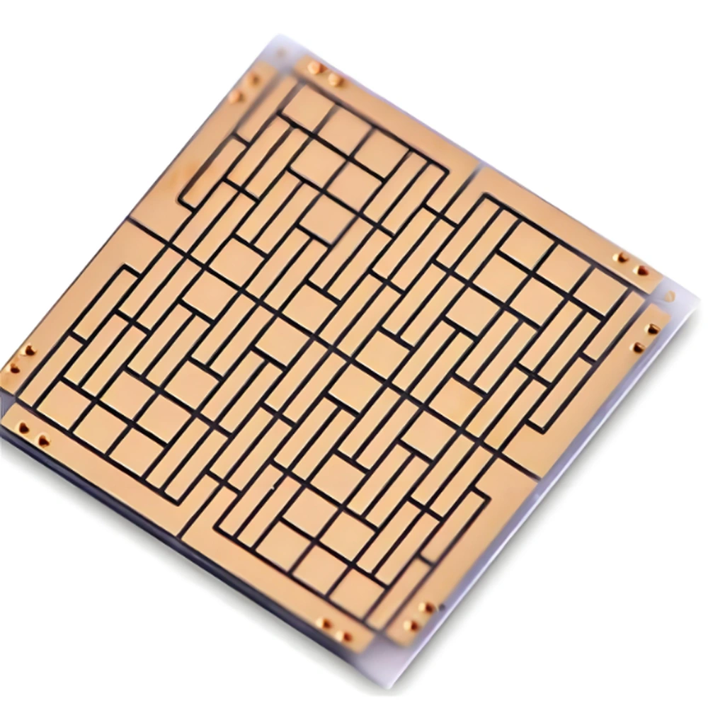
AlN DPC substrates combine plated copper circuitry with an aluminum nitride insulating heat path.
The patterned copper connects devices and attachment pads, while AlN carries heat through the ceramic to the cooling interface. This construction is useful for compact LED, laser and power-electronic packages.
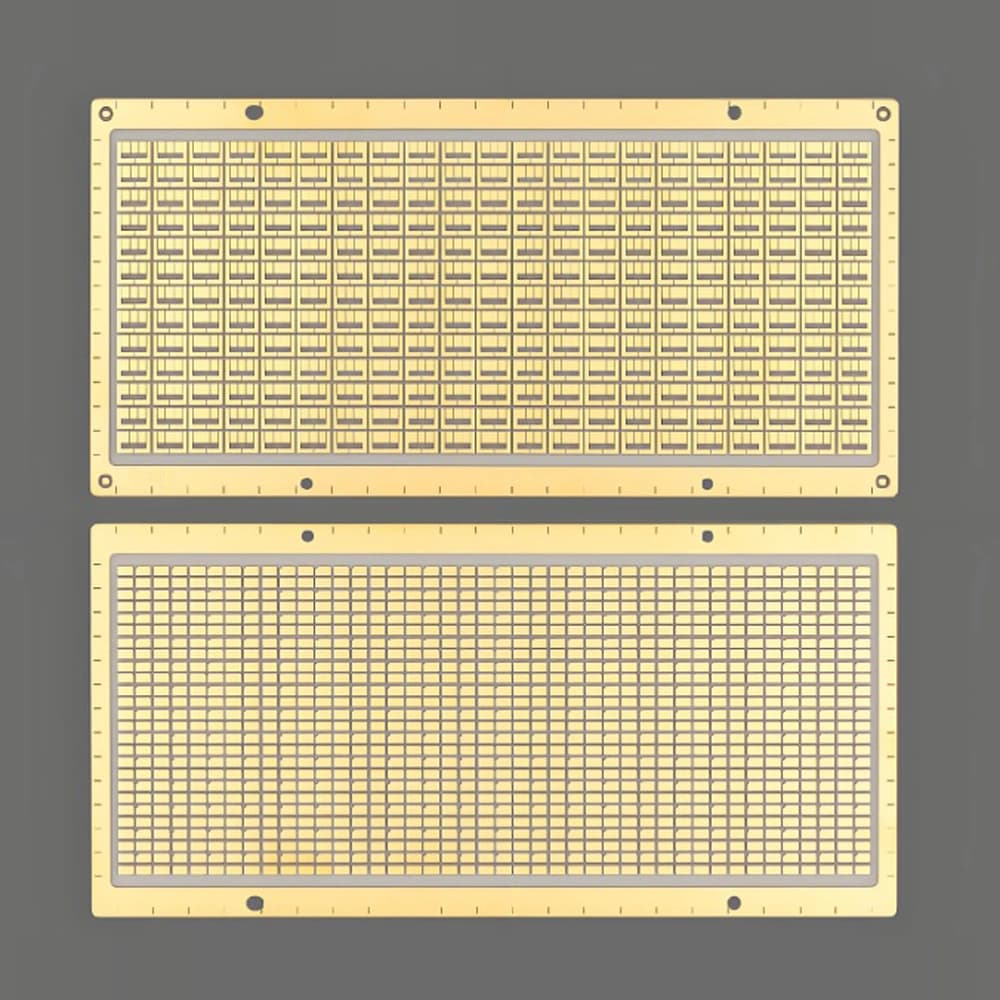
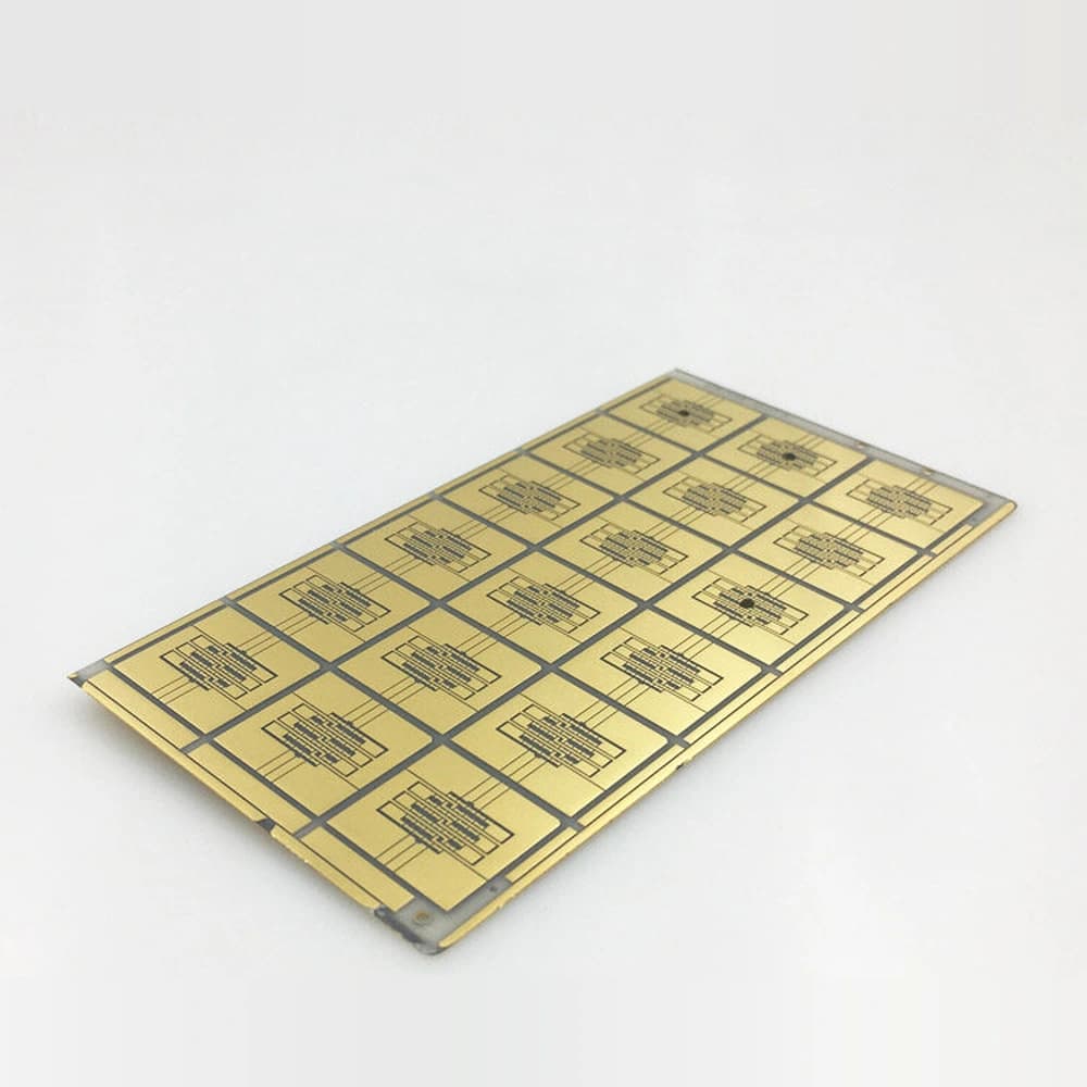
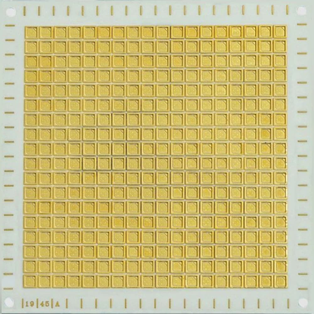
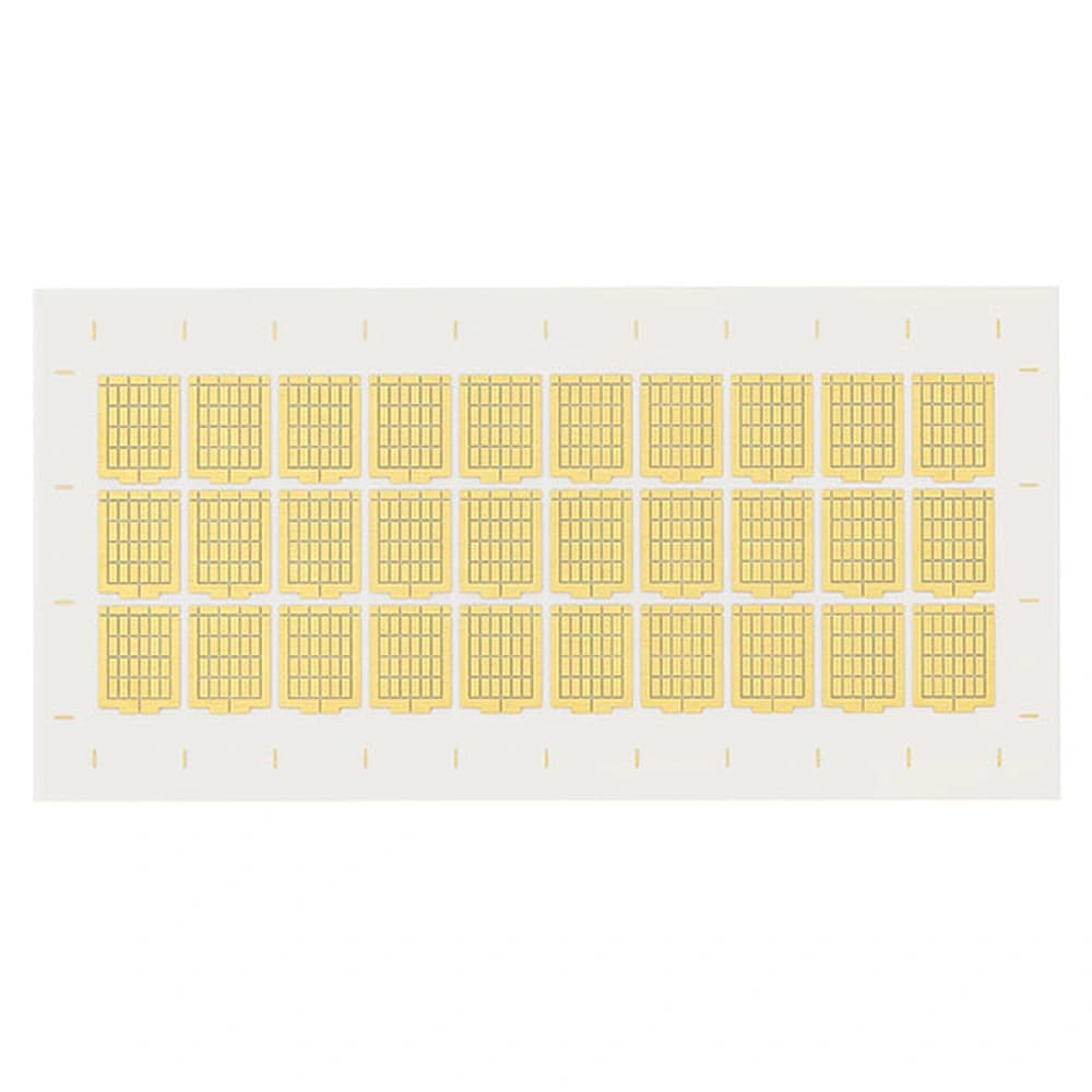
Fine plated copper on AlN is illustrated. Copper thickness, conductor spacing, adhesion and surface finish require drawing and process review.
Product Advantages
- Plated copper connects device pads and traces on an insulating AlN carrier.
- AlN provides a ceramic heat path beneath concentrated electronic devices.
- Photolithographic patterning integrates attachment areas with the package layout.
Typical Applications
- LED and Laser Packages: copper pads support device attachment over an AlN heat path.
- Power Electronics: patterned conductors and AlN insulation share a compact carrier.
Technical Data
95% AlN Substrate Properties
| Property | 95% AlN typical value | Condition / method |
|---|---|---|
| AlN content (%) | 95 | — |
| Density (g/cm³) | ≥3.3 | — |
| Flexural strength (MPa) | ≥400 | — |
| Thermal conductivity (W/(m·K)) | ≥170 | Room temperature |
| Relative permittivity | 8–10 | 1 MHz; room temperature |
| Dielectric loss tangent | ≤0.0003 | 1 MHz; room temperature |
| Dielectric strength (kV/mm) | 17 | — |
| Volume resistivity (Ω·cm) | ≥10¹⁴ | — |
Typical Construction Parameters
| Construction item | Typical configuration | Applicable condition |
|---|---|---|
| Ceramic base | Aluminum nitride (AlN) | Surface preparation dependent |
| Copper thickness | 10–130 µm | Plated thickness and pattern evaluated together |
| Line / space | Layout-dependent | Copper thickness, plating distribution and pattern geometry |
| Holes / vias | Laser holes and selected plated features | Aspect ratio and registration dependent |
| Surface finish | Ni/Au, Ni/Pd/Au or Ag examples | Finish stack matched to the attachment process |
How to Read the Parameters
- Copper thickness and line/space
Pattern feasibility depends on the finished copper thickness and geometry.
Specify: Thickness distribution, minimum gap, pad shape and registration basis.
- Surface condition
Bare ceramic, plated copper and pad finish are distinct surfaces.
Specify: Functional face, roughness parameter, cleanliness and finish composition/thickness.
- Resistivity and isolation
Volume resistivity uses Ω·cm or Ω·m; finished-circuit insulation resistance uses Ω.
Specify: Temperature, humidity, voltage, time and test geometry.
- RF material and circuit data
Permittivity and loss require frequency and test conditions.
Specify: Operating band, method, conductor stack and circuit-level acceptance.
- Adhesion
Peel in N/mm is not tensile or shear strength in MPa.
Specify: Test mode, geometry, rate, specimen preparation and failure location.
DPC: build and pattern the copper stack
DPC forms patterned copper on ceramic using an adhesion/seed stack, photolithography and electroplating. This substrate-metallization route is separate from any later functional thin-film processing, die attachment or package sealing.

Application Conditions & Design Review
Place heat sources and copper together
AlN DPC is a candidate for compact packages needing both patterned copper and an insulating heat-transfer path. Review the local die footprint and backside interface rather than only the overall plate size.
Select a finish for the attachment method
Soldering, wire bonding and later film processing may require different pad conditions. Define the interface needed by the selected assembly process before choosing the final metal finish.
Ceramic and copper
Select the ceramic grade and thickness with the plated-copper geometry and heat-source footprint.
Thin-film integration
Identify which resistor, conductor, dielectric or passivation layers will be added after DPC, and review their process compatibility.
Double-sided and via functions
Define each face and any vertical connections explicitly; rear copper does not imply through-hole connectivity.
RF requirements
Specify the operating band and finished-circuit requirements, not merely a low-frequency ceramic dielectric value.
Send With Your Drawing
- AlN grade, finished geometry and top/bottom copper artwork and thickness.
- Heat-source positions and die-attach/cooling interface requirements.
- Pad finish, interconnect method and electrical isolation criteria.
Include the drawing revision, sample and production quantities, and required inspection documents.
Define Acceptance Before Production
- Check pattern dimensions, copper thickness, surface condition and specified geometry.
- Qualify attachment integrity and thermal/electrical behavior in the intended package.
Agree the test methods, sampling plan, acceptance limits and required reports before production.
Available Forms & Processing
Product-specific geometry and processing features.
- Selected AlN grade, ceramic thickness and plated copper thickness identified together.
- Trace spacing, pad geometry and plating build-up coordinated within one pattern.
- Surface finish and rear thermal-contact area defined for the attachment system.
Engineering Questions
Does a high-conductivity AlN grade guarantee low package temperature?
No. Heat-source area, copper layout, attachment quality and cooling also determine device temperature. Assess the complete thermal path.
How should the DPC surface finish be selected?
Start with the attachment or downstream film process. Specify finish composition and thickness, pad areas, cleanliness and oxidation protection, then confirm compatibility with the intended soldering, bonding or deposition sequence.
Does a dielectric constant measured at 1 MHz prove microwave performance?
No. Use material data at relevant frequencies and evaluate the actual conductor geometry, finish, interconnections and completed circuit.
Packaging & Shipping
Packaging is selected for master cards, individual units and copper surface condition.
| Item | Details |
|---|---|
| Packaging approach | Packaging is selected for master cards, individual units and copper surface condition. |
| Protection methods | Individual separation; Anti-scratch surface protection; Rigid trays or master-card frames; Copper corrosion protection where appropriate; Inner box and export carton; Wooden case when required |
| MOQ reference | 10 pieces or one master-card equivalent |
| Lead-time references | DPC: 5-8 weeks |
| Payment terms | T/T / Western Union / PayPal; 50% advance payment, 50% balance before shipment |
| Shipping methods | Sea freight / Air freight / Door-to-door courier |

Related Ceramic Substrate Products
Compare related ceramic substrate materials and metallization routes within the same product family.