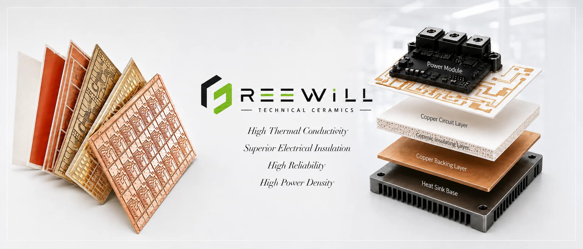
FreeWill Material Technical Ceramics

Ceramic Substrates

Ceramic Substrate Product Finder

Filter all substrate products on one page.

Combine material, process and application filters, or search by a product name or use case. Filters within one group are additive; different groups narrow the result together.

37 matching products

Filter Ceramic Substrates
Material
Process / Construction
Application Function

Filtered Product Portfolio

Products matching your selection

Ceramic Insulating Substrates for Thermoelectric Modules product overview

96% Alumina · Bare / Standard

Ceramic Insulating Substrates for Thermoelectric Modules

96% alumina insulating substrates for thermoelectric module assembly, reviewed for outline, thickness, surface condition and circuit requirements.

Typical applications

Thermoelectric Modules · Electronic Insulation

View Product Details
Laser-Drilled Alumina Ceramic Substrates product overview

96% Alumina · Laser / Drilling

Laser-Drilled Alumina Ceramic Substrates

96% alumina substrates with drawing-defined laser holes for electronic circuits, packaging and precision assembly.

Typical applications

Electronic Packaging · Circuit Substrates

View Product Details
Large-Size Low-Warpage Alumina Ceramic Substrates product overview

96% Alumina · Bare / Standard

Large-Size Low-Warpage Alumina Ceramic Substrates

Large-format 96% alumina substrate configurations reviewed for thickness, flatness, warpage and downstream processing.

Typical applications

Large Electronic Panels · Industrial Electronics

View Product Details
Laser-Scribed Alumina Substrates for Integrated Circuits product overview

96% Alumina · Laser / Drilling

Laser-Scribed Alumina Substrates for Integrated Circuits

96% alumina substrates with controlled laser scribing for circuit-panel separation and integrated-circuit production.

Typical applications

Integrated Circuits · Hybrid Circuits

View Product Details
Alumina Substrates for Thin-Film Integrated Circuits product overview

96% Alumina · Bare / Standard

Alumina Substrates for Thin-Film Integrated Circuits

Surface-controlled alumina substrates for thin-film integrated circuits and precision electronic packaging.

Typical applications

Thin-Film Circuits · Microelectronics

View Product Details
Alumina Ceramic Substrates for Optoelectronic Transceiver Modules product overview

99.6% Alumina · Bare / Standard

Alumina Ceramic Substrates for Optoelectronic Transceiver Modules

High-purity alumina substrates for optoelectronic transceiver packaging, precision circuits and electrically insulating carriers.

Typical applications

Optical Transceivers · Optoelectronic Packaging

View Product Details

Material Selection

Compare the role of each base ceramic.

These qualitative selection cues support early sourcing discussions. Final selection depends on the complete electrical, thermal, mechanical and processing requirements.

Cost-effective and established

Alumina

A mature electronic substrate material with electrical insulation and broad processing availability.

  • Electrical insulation
  • Broad processing availability

Thermal management focus

Aluminum Nitride

Considered where higher thermal management capability and electrical insulation are both important.

  • Electrical insulation
  • Power electronics relevance

Mechanical reliability focus

Silicon Nitride

Considered for mechanical reliability and demanding thermal-cycling conditions in power-module applications.

  • Mechanical reliability
  • Thermal-cycling relevance

Selection Guide

Compare ceramic substrate options at a glance.

Use the two tables to compare copper-attachment technologies and ceramic base materials. On smaller screens, swipe horizontally to view every column.

DBC vs DPC vs AMB
FactorDBCDPCAMB
ProcessDirect-bonded copper foilSeed deposition, plated copper and patterningCopper joined by active-metal braze
Ceramic Base96% Al2O3 or AlN96% / 99.6% Al2O3 or AlNSi3N4 primary; selected AlN
Copper SystemThick bonded foilThin-to-medium controlled plated copperThick brazed copper
Copper Thickness0.10-0.30 mm standard range10-130 micrometers; 30-100 micrometers typical0.30 / 0.40 / 0.50 / 0.80 mm references
Circuit PrecisionMediumHighest of the threeMedium; power-layout oriented
Thermal PerformanceStrong; AlN option lowers thermal resistanceGood for localized heat and precision packagesStrong system performance with high reliability
Mechanical ReliabilityGood; layout and ceramic dependentBest suited to compact, light-copper circuitsHighest severe-cycle positioning
Automotive SuitabilityMedium-to-high by designSelected sensors and optoelectronicsVery high positioning
Power ElectronicsHighLow-to-medium depending on copper and currentVery high
Fine CircuitsMediumHighLow-to-medium
Typical ApplicationsIGBT/MOSFET modules, drives and invertersLED, laser, LiDAR, optical and RF packagesEV traction, SiC modules and automotive inverters
MOQ5 pcs or one master-card equivalent10 pcs or one master-card equivalent5 pcs or one master-card equivalent
Lead Time5-9 weeks5-8 weeks6-10 weeks
Ceramic Base Material Comparison
PropertyAluminaAluminum NitrideSilicon Nitride
Thermal ConductivityAbout 20-30 W/(m K) typical, grade dependentAbout 170 W/(m K) typical; higher grades availableAbout 80-90 W/(m K) typical for power-substrate grades
Electrical InsulationStrong and widely establishedStrong with high heat-transfer capabilityStrong for power-module isolation
Mechanical StrengthGood general-purpose substrate strengthGood, but more brittle than Si3N4Highest strength positioning of these substrate bases
Fracture ToughnessModerateLower than Si3N4Highest of these three substrate bases
Thermal-Cycle ReliabilityGood when layout and copper are balancedGood thermal path; stress design remains importantBest positioning for severe thermal cycling
Cost PositionMost economical and establishedPremium thermal-management materialPremium reliability-focused material
Typical Copper RoutesDBC, DPC, thick film and thin filmDBC, DPC and selected AMBAMB priority; selected other routes by review
Recommended ApplicationsGeneral electronics, thick-film circuits and cost-sensitive modulesHigh heat-flow power electronics, LEDs and lasersEV inverters, SiC modules and high-reliability power cycling

Values and rankings are typical selection references, not guaranteed order specifications. Confirm material grade, geometry, copper thickness, circuit layout, finish, assembly process and test method during RFQ review.

Processing Capabilities

Drawing-based substrate processing options.

Processing routes are reviewed for the selected material, substrate geometry, feature pattern and inspection requirements.

  • Laser Cutting
  • Laser Drilling
  • Laser Scribing
  • Precision Machining
  • Polishing
  • Metallization
  • Custom Shapes

Typical Applications

Electronic and thermal-management application directions.

Application requirements guide material-family and processing review; the examples below are sourcing contexts rather than fixed specifications.

  • Power Electronics
  • LED Packaging
  • Thin Film Circuits
  • Thick Film Circuits
  • Sensors
  • Optoelectronics
  • Thermal Management
  • Electronic Modules

Engineering RFQ

Tell us what the substrate must do.

Provide the drawing, dimensions, quantity and application requirements so the team can review material and processing options before quotation.

Engineering RFQ

Tell us what the component must do.

All fields are required. Provide practical operating details so our team can review the material and manufacturing requirements.

Your request will be reviewed by our team before a technical or commercial response is issued.