
FreeWill Material Technical Ceramics

Material-Specific Product Family

Aluminum Nitride Ceramic Substrates

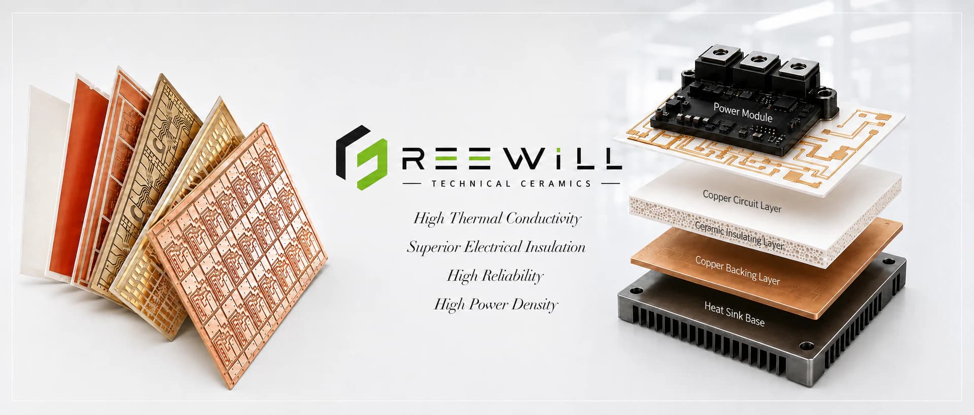
FreeWill Material ceramic substrates and power module thermal-management assembly

High-thermal-conductivity AlN substrates for electrically insulating heat transfer in power electronics, optoelectronics and semiconductor packaging.

Material & Process Filter

Filter compatible substrate processes.

Only technically compatible routes are shown. Select one or more processes to compare matching products; clear the selection to return to the base-material portfolio.

Compatible process routes

Product Family Portfolio

Aluminum Nitride Ceramic Substrate Products

Select a product route for detailed application and drawing-review guidance.

7 products

Aluminum Nitride Ceramic Substrates product overview

Aluminum Nitride Ceramic Substrate Products

Aluminum Nitride Ceramic Substrates

Bare and drawing-processed AlN substrates for electrically insulated heat spreading in power and optoelectronic assemblies.

Typical application directions

Power Electronics · Thermal Management

View Product Details
Aluminum Nitride Ceramic Substrates for Thick-Film Circuits product overview

Aluminum Nitride Ceramic Substrate Products

Aluminum Nitride Ceramic Substrates for Thick-Film Circuits

AlN substrates prepared for thick-film circuit processing where thermal management and electrical insulation are required.

Typical application directions

Thick-Film Circuits · Hybrid Microelectronics

View Product Details
Mirror-Grade Double-Sided Polished AlN Ceramic Substrates product overview

Aluminum Nitride Ceramic Substrate Products

Mirror-Grade Double-Sided Polished AlN Ceramic Substrates

Double-sided polished AlN substrates for precision thin-film, optical and microelectronic assembly processes.

Typical application directions

Thin-Film Circuits · Optoelectronic Packaging

View Product Details
AlN Ceramic Substrates for Thin-Film Circuits product overview

Aluminum Nitride Ceramic Substrate Products

AlN Ceramic Substrates for Thin-Film Circuits

Surface-controlled AlN substrates for thin-film circuits and compact high-heat-flux electronic packages.

Typical application directions

Thin-Film Circuits · High-Heat-Flux Electronics

View Product Details
Aluminum Nitride Ceramic Substrates for IGBT Power Modules product overview

Aluminum Nitride Ceramic Substrate Products

Aluminum Nitride Ceramic Substrates for IGBT Power Modules

AlN substrates for electrically insulated heat transfer in IGBT power-module assemblies.

Typical application directions

IGBT Power Modules · Power Inverters

View Product Details
Laser Precision-Machined Aluminum Nitride Substrates product overview

Aluminum Nitride Ceramic Substrate Products

Laser Precision-Machined Aluminum Nitride Substrates

AlN substrates with drawing-defined laser outlines, holes and precision features for electronic assembly.

Typical application directions

Precision Electronic Packaging · Custom Circuits

View Product Details

Thermal Conductivity Options

Select the AlN grade around the thermal design.

Thermal conductivity varies with grade and formulation. Higher-conductivity options are selected when thermal modeling justifies them.

About 170 W/m·K typical

Standard AlN Grade

A high-conductivity electrically insulating substrate for mainstream thermal-management designs.

  • Balanced performance
  • Broad power and optoelectronic use

200–230 W/m·K class

Higher-Conductivity AlN

Optional grades for applications requiring lower ceramic thermal resistance.

  • Grade-dependent availability
  • Selected after thermal review

Processing Capabilities

Precision processing for heat-flow and assembly requirements.

Geometry and finish are reviewed against thickness, thermal-conductivity grade and downstream metallization.

  • Laser Cutting
  • Laser Drilling
  • Laser Scribing
  • Grinding
  • Lapping
  • Polishing
  • Metallization
  • Custom Geometry

Typical Properties

AlN performance for thermal-management selection.

Values are typical references and depend on grade and test method.

PropertyWebsite referenceCondition
Density3.26–3.33 g/cm³ typicalGrade dependent
Flexural strength330–450 MPa typicalMethod and grade dependent
Thermal conductivity170 W/m·K typical standard gradeHigher-conductivity 200–230 W/m·K class options
CTE4.5–4.7 × 10⁻⁶/K typicalTemperature range dependent
Dielectric constantAbout 8.5–9.0 at 1 MHzGrade and method dependent
Volume resistivity≥10¹³ Ω·cm typicalAt room temperature
Dielectric strength>15 kV/mm typicalDepends on thickness and test method

Available Specifications

Common formats with drawing-based limits.

Dimensions, tolerances and surface requirements depend on grade, thickness and processing.

ItemWebsite referenceCondition
Thickness0.38–1.5 mm standard commercial rangeNot every size and grade combination
Size50.8–127 mm square standard references; approximately 140 × 190 mm by reviewSubject to grade and drawing review
Dimensional tolerance±0.2 mm standard referenceTighter tolerances may be available
Flatness / warpage≤0.2% of length general referenceDepends on dimensions and thickness
Surface roughnessAs-fired Ra typically 0.2–0.6 µmLapped and polished surfaces available
ProcessingCutting, drilling, scribing, lapping, polishing and metallizationSubject to drawing review

Product Solutions

Bare, processed and metallization-ready AlN substrates.

Product forms are quoted to drawing without implying a separate SKU page.

  • Standard AlN Substrates
  • Higher-Conductivity AlN Substrates
  • Laser-Processed AlN Substrates
  • Polished AlN Substrates
  • Metallization-Ready AlN Substrates

Applications

Use AlN when heat flow becomes the limiting factor.

AlN retains electrical insulation while reducing thermal resistance through the ceramic layer compared with alumina.

  • IGBT Modules
  • MOSFET Modules
  • SiC Power Modules
  • GaN Power Devices
  • High-Power LEDs
  • Laser Diodes
  • RF / Microwave Electronics
  • Semiconductor Packaging
  • EV Power Electronics
  • Industrial Inverters
  • Thermal Management

Selection Guidance

AlN is an independent thermal substrate platform.

Choose by thermal resistance, assembly process and mechanical duty rather than treating AlN as simply a better alumina.

PriorityRecommended directionWhy
Cost and mature processingAluminaEstablished and economical
Highest bulk thermal conductivityAluminum NitrideEfficient electrically insulating heat path
Severe thermal cycling and toughnessSilicon NitrideHigher fracture toughness and reliability

Custom Manufacturing

Configure AlN around the heat-flow path.

Custom outlines and surfaces are reviewed with the grade and assembly process.

  • Custom laser-cut outlines
  • Holes, slots and scribe lines
  • Grinding and thickness control
  • Lapped and polished surfaces
  • DPC, DBC/AMB, thick-film and thin-film options
  • Drawing-based inspection

Quality & Inspection

Verify the substrate features that control assembly.

Inspection and documentation are agreed during quotation and available on request.

  • Grade and thermal-conductivity review
  • Dimensions and thickness
  • Flatness and warpage
  • Surface roughness and visual inspection
  • Laser feature and hole position
  • Metallization inspection

Packaging & Shipping

Protect AlN edges and prepared surfaces.

AlN substrates receive individual separation and surface protection appropriate to the finish.

  • Individual separation
  • Anti-scratch interlayers
  • Rigid trays or foam protection
  • Moisture protection where appropriate
  • Inner box and export carton
  • Wooden case when required

Ordering Information

MOQ and typical lead time.

Typical lead times depend on grade availability, drawing, quantity, processing and inspection requirements.

Recommended MOQ

5 pieces

Bare substrates

3–5 weeks

Precision processing

4–6 weeks

Metallized

5–9 weeks

FAQ

Questions buyers commonly ask.

Practical sourcing questions for material selection, processing and ordering.

Is every AlN substrate rated at 230 W/m·K?

No. The standard website position is about 170 W/m·K typical. The 200–230 W/m·K class describes optional higher-conductivity grades.

Why choose AlN instead of alumina?

Choose AlN when heat must pass through an electrically insulating ceramic with substantially lower thermal resistance.

Can AlN be laser processed and polished?

Yes. Geometry, chipping criteria, thickness and surface requirements are reviewed together.

What is the MOQ and lead time?

Recommended MOQ is 5 pieces. Typical lead time is 3–5 weeks bare, 4–6 weeks precision processed and 5–9 weeks metallized, depending on specification and quantity.

Material reference

Review AlN material properties and selection context separately from the product-family offer.

Learn About Aluminum Nitride Ceramic

What to Specify for RFQ

Define the grade, geometry and assembly requirements.

Thermal-conductivity class and surface condition are essential to a useful AlN quotation.

  • Thermal-conductivity class
  • Length × width × thickness
  • Drawing and quantity
  • Tolerance and flatness
  • Surface finish / roughness
  • Hole and scribing pattern
  • Metallization stack
  • Operating environment
  • Inspection and packaging

Engineering RFQ

Tell us what the substrate must do.

Provide the drawing, dimensions, quantity and application requirements so the team can review material and processing options before quotation.

Engineering RFQ

Tell us what the component must do.

All fields are required. Provide practical operating details so our team can review the material and manufacturing requirements.

Your request will be reviewed by our team before a technical or commercial response is issued.