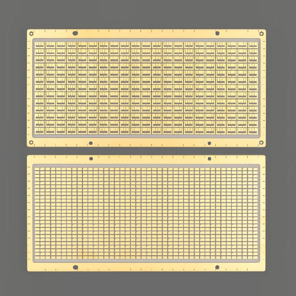
Double-Sided Copper-Clad DPC Metallized Substrates
Double-sided DPC substrates for compact circuit layouts and controlled plated-copper integration.
View product
DPC Product Family

DPC ceramic substrates carry patterned plated copper on an insulating alumina or aluminum nitride base.
DPC ceramic substrates carry patterned plated copper on an insulating alumina or aluminum nitride base. Seed-layer deposition, photolithography and copper plating form conductors and connection pads for compact electronic packages.
Copper thickness, line spacing and plating distribution are linked features of one circuit layout. Double-sided copper and plated through-connections are separate options; a via requires its own defined hole and metallization construction.
Product Family Portfolio
Select a product route for detailed application and drawing-review guidance.
5 products
Double-sided DPC substrates for compact circuit layouts and controlled plated-copper integration.
View product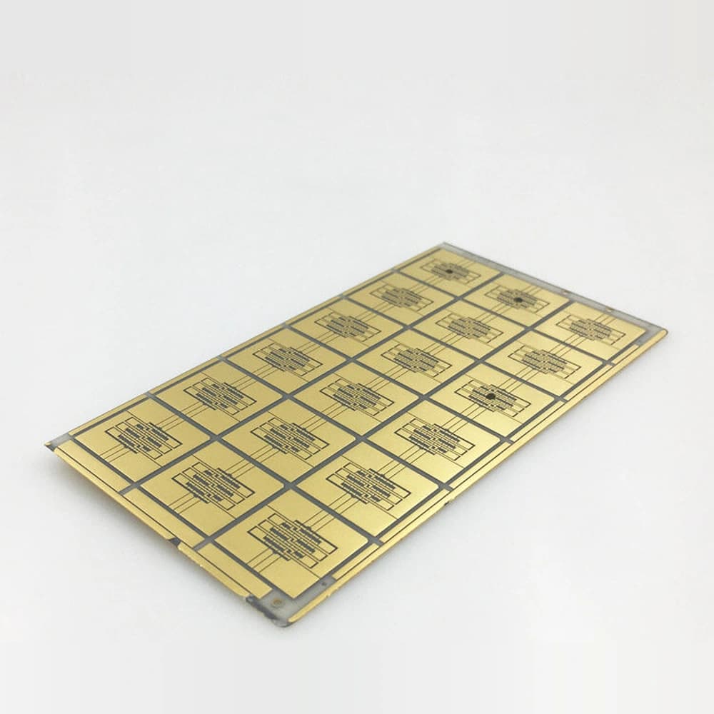
Fine-pattern DPC substrates for precision electronic packages, with conductor-stack review to distinguish plated copper from other thin-film systems.
View product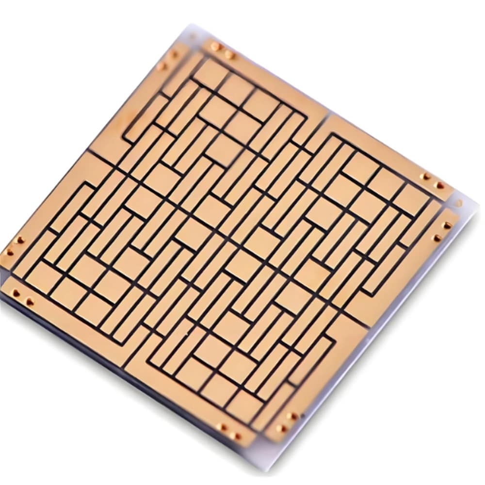
AlN DPC substrates combining controlled plated copper with an electrically insulating thermal path.
View product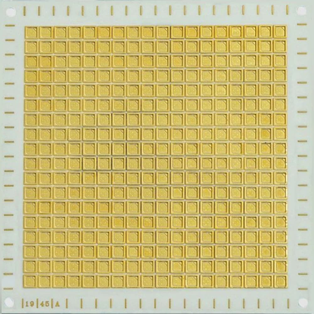
Alumina DPC substrates for fine copper patterns, electronic packaging and drawing-defined circuit layouts.
View product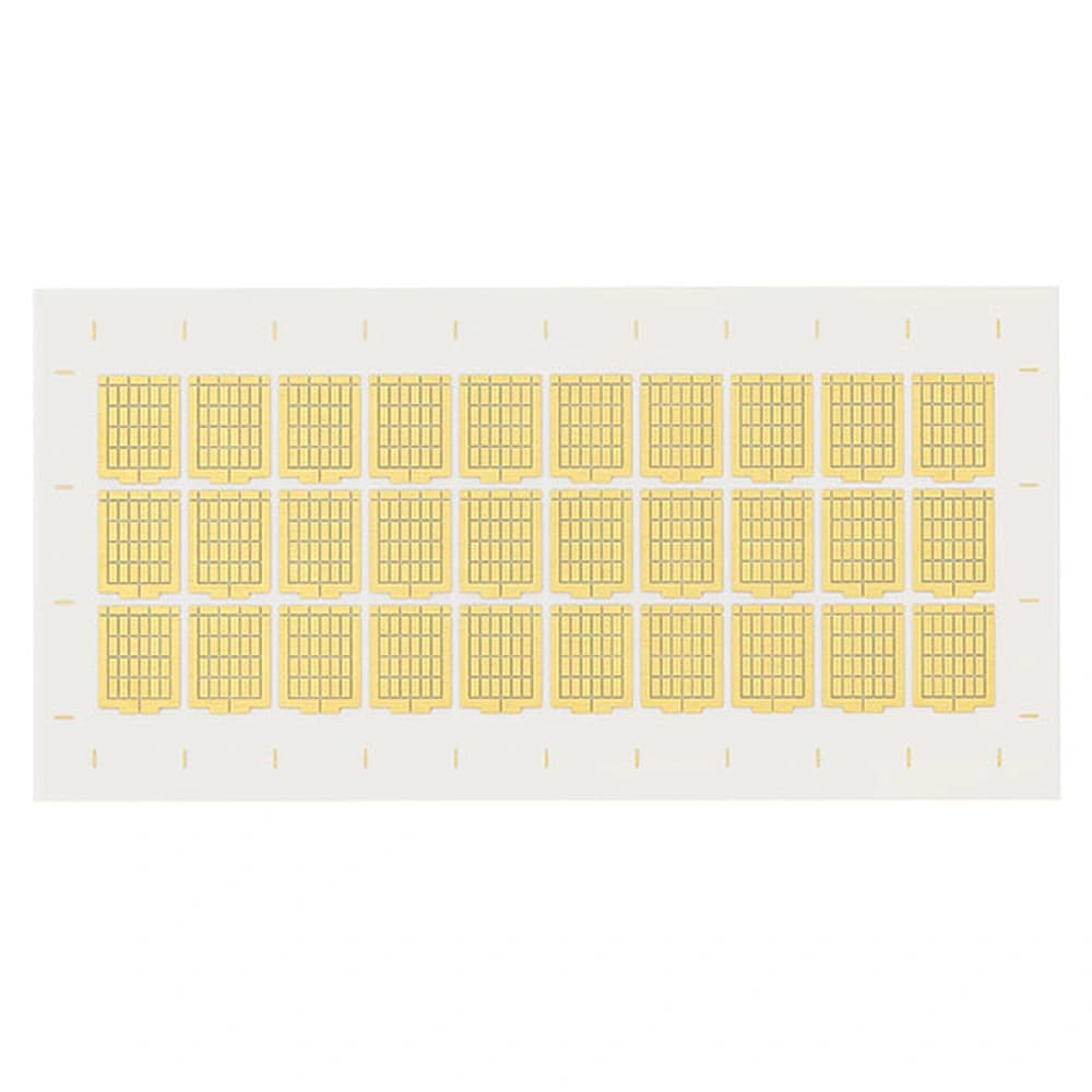
DPC metallized ceramic substrates for thermoelectric cooling-chip circuits and compact heat-management assemblies.
View productPatterned pads and conductors support compact optical, electronic and sensor packages.
Construction Parameters
| Construction item | Typical configuration | Applicable condition |
|---|---|---|
| Ceramic base | 96% / 99.6% Al2O3 or AlN | Surface preparation dependent |
| Copper thickness | 10–130 µm | Plated thickness and pattern evaluated together |
| Line / space | Layout-dependent | Copper thickness, plating distribution and pattern geometry |
| Holes / vias | Laser holes and selected plated features | Aspect ratio and registration dependent |
| Surface finish | Ni/Au, Ni/Pd/Au or Ag examples | Finish stack matched to the attachment process |
Construction Selection
| Element | Function | Construction definition |
|---|---|---|
| Ceramic | Electrical insulation and heat path | Material grade, thickness and functional surface |
| Copper | Current paths, attachment and heat spreading | Top / bottom thickness, pattern and isolation gaps |
| Interface and finish | Copper attachment and subsequent assembly | Seed / plated layers, distribution and attachment finish |
| Thermal / electrical assessment | Performance of the complete stack | Layer geometry, test method, operating conditions and interfaces |
Product configuration
Processing defines the conductor geometry and the surfaces used in assembly.
Configuration Scope
Ceramic base, copper system, circuit layout, finish and qualification requirements are reviewed together.
Quality & Inspection
Inspection and documentation are available on request and defined during quotation.
Ordering Information
MOQ and lead time depend on ceramic base, copper layout, finish, panel utilization, quantity and qualification requirements.
Recommended MOQ
10 pieces or one master-card equivalent
DPC
5-8 weeks
FAQ
Practical sourcing questions for material selection, processing and ordering.
Yes. Alumina and AlN are common for DBC/DPC, while Si3N4 is the priority AMB base for high-reliability power modules.
Copper thickness, plating distribution, feature registration and the pattern geometry are specified together.
Provide ceramic and copper thickness, metallization route, circuit file, finish, electrical or reliability criteria, quantity and assembly process.
Packaging & Shipping
Packaging is selected for master cards, individual units and copper surface condition.
What to Specify for RFQ
Metallized substrates require more than an outline drawing.
Engineering RFQ
Provide the drawing, dimensions, quantity and application requirements so the team can review material and processing options before quotation.