Ceramic Insulating Substrates for Thermoelectric Modules
96% alumina insulating substrates for thermoelectric module assembly, reviewed for outline, thickness, surface condition and circuit requirements.
View product

Ceramic substrates provide electrical insulation, mechanical support and a heat-transfer path for electronic assemblies.
Ceramic substrates provide electrical insulation, mechanical support and a heat-transfer path for electronic assemblies. Bare alumina, aluminum nitride and silicon nitride plates form the ceramic base; DBC, DPC and AMB add defined copper circuit structures.
Choose the ceramic material and the delivery construction separately. Polishing, laser holes and scribe lines define the blank's geometry and surface, while copper thickness, pattern and finish define a copper-clad circuit substrate. Co-fired HTCC and LTCC are separate multilayer routes.
Ceramic Substrate Product Finder
Combine material, process and application filters, or search by a product name or use case. Filters within one group are additive; different groups narrow the result together.
37 matching products
Filtered Product Portfolio
96% alumina insulating substrates for thermoelectric module assembly, reviewed for outline, thickness, surface condition and circuit requirements.
View product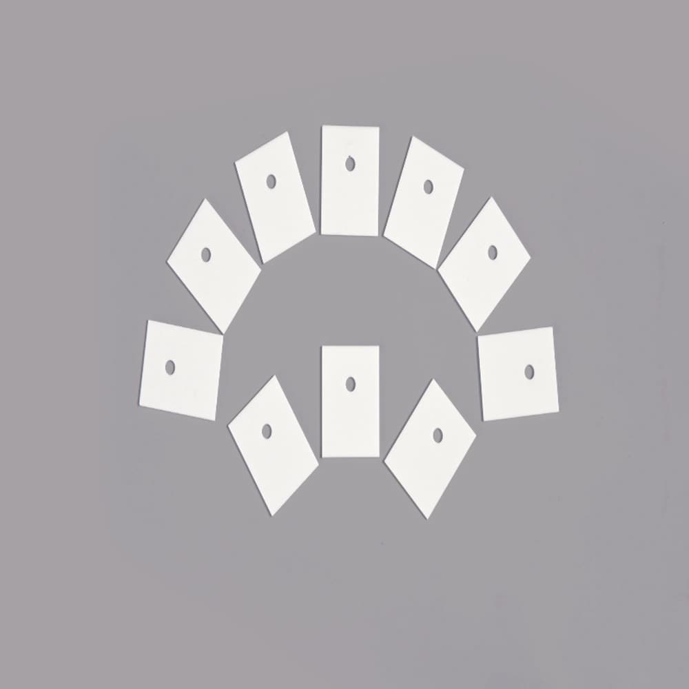
96% alumina substrates with drawing-defined laser holes for electronic circuits, packaging and precision assembly.
View product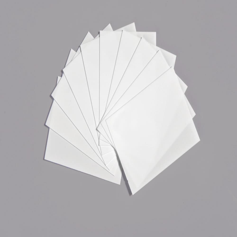
Large-format 96% alumina substrate configurations reviewed for thickness, flatness, warpage and downstream processing.
View product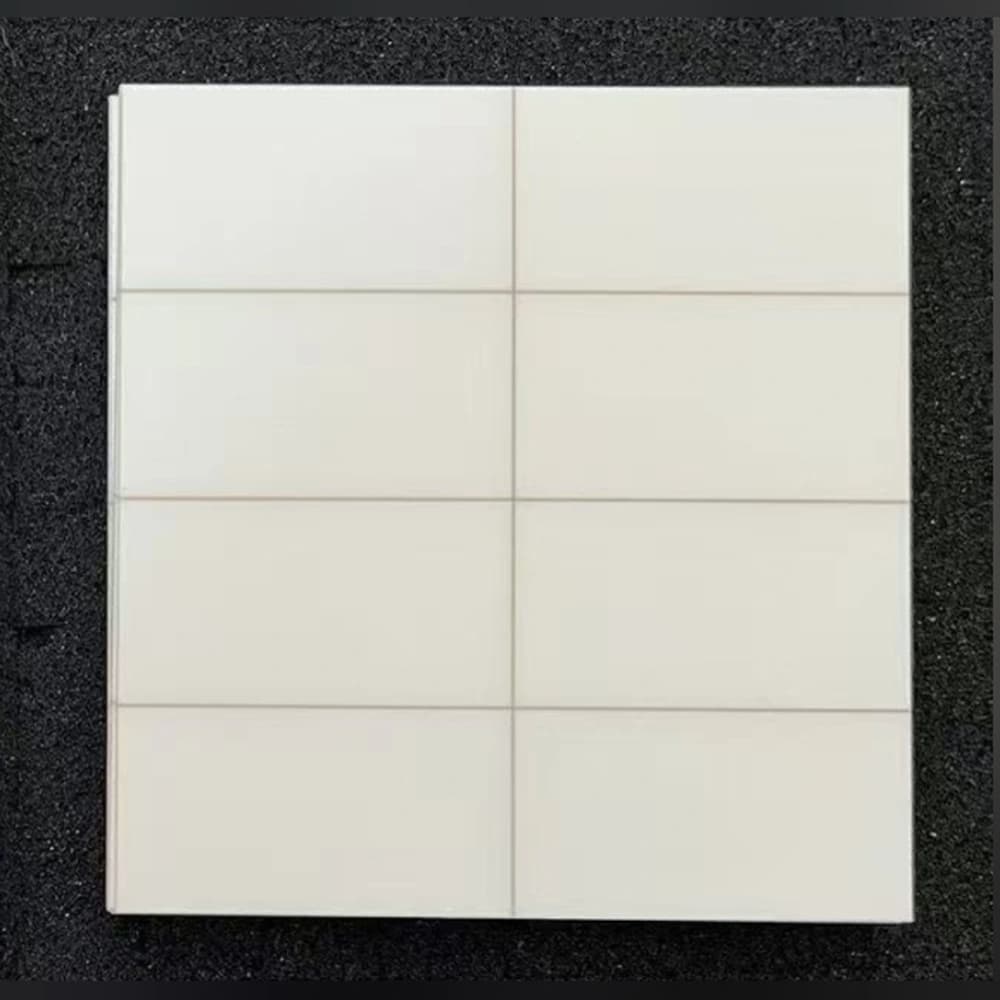
96% alumina substrates with controlled laser scribing for circuit-panel separation and integrated-circuit production.
View product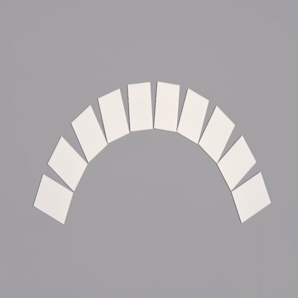
Surface-controlled alumina substrates for thin-film integrated circuits and precision electronic packaging.
View product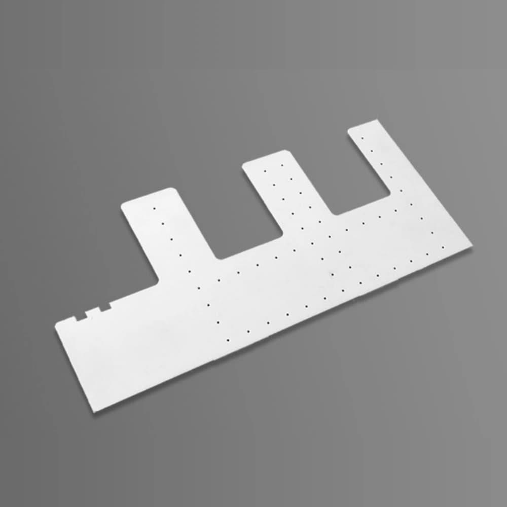
High-purity alumina substrates for optoelectronic transceiver packaging, precision circuits and electrically insulating carriers.
View productCeramic and circuit construction are selected for the role within each assembly.
Selection Guide
Use the two tables to compare copper-attachment technologies and ceramic base materials. On smaller screens, swipe horizontally to view every column.
| Factor | DBC | DPC | AMB |
|---|---|---|---|
| Process | Direct-bonded copper foil | Seed deposition, plated copper and patterning | Copper joined by active-metal braze |
| Ceramic Base | 96% Al2O3 or AlN | 96% / 99.6% Al2O3 or AlN | Si3N4, AlN or alumina; material-specific braze stack |
| Copper System | Bonded foil | Patterned plated copper | Brazed copper |
| Copper Thickness | 0.10–0.30 mm; matched ceramic / copper stack | 10–130 µm; plating and pattern evaluated together | 0.30 / 0.40 / 0.50 / 0.80 mm; selected AMB stacks |
| Circuit Geometry | Etch profile, copper thickness and isolation gap | Plating distribution, copper thickness and feature registration | Copper thickness, braze system and pattern coverage |
| Heat Path | Ceramic, copper, bonded interface and cooling contact | Ceramic, plated copper and attachment interfaces | Ceramic, copper, braze interface and cooling contact |
| Mechanical Assessment | Ceramic grade, copper balance and mounting stress | Feature geometry, plated-layer distribution and attachment stress | Ceramic / braze / copper stack and operating cycle |
| Automotive Applications | Defined power-circuit and qualification requirements | Defined sensor or optoelectronic package requirements | Defined inverter / power-module and qualification requirements |
| Power Electronics | Current paths and attachment pads in bonded copper | Current capacity linked to plated cross-section and layout | Current paths and attachment pads in brazed copper |
| Fine Circuits | Etched conductor geometry | Photolithographically defined plated geometry | Patterned copper with braze and clearance requirements |
| Typical Applications | IGBT/MOSFET modules, drives and inverters | LED, laser, LiDAR, optical and RF packages | EV traction, SiC modules and automotive inverters |
| MOQ | 5 pcs or one master-card equivalent | 10 pcs or one master-card equivalent | 5 pcs or one master-card equivalent |
| Lead Time | 5-9 weeks | 5-8 weeks | 6-10 weeks |
| Property | Alumina — 708 S / 710 C | 95% Aluminum Nitride | Si₃N₄ — Sinalit substrate |
|---|---|---|---|
| Thermal Conductivity (W/(m·K); room temperature) | 96% (708 S): 24; 99.6% (710 C): ≥25 | ≥170 | 90 |
| Thermal-conductivity test conditions | Room temperature; DIN EN 821-2; ±10% measurement tolerance | Room temperature | Room temperature; DIN EN 821-2; ±10% measurement tolerance |
| Electrical Insulation | Insulating carrier for film circuits and electronic packages | Insulating ceramic heat path | Insulating ceramic in power-module structures |
| Mechanical Behavior | Rigid support; grade, geometry and mounting matter | Rigid support; thickness, edges and mounting matter | Strength and fracture toughness support stress-bearing ceramic layers |
| Fracture / Edge Design | Edges, holes and support spacing define stress concentrations | Edges, holes and support spacing define stress concentrations | Toughness is considered with ceramic geometry and bonded copper |
| Thermal-Cycle Assessment | Copper balance, interfaces and ceramic geometry | Heat path, expansion mismatch and interface stress | Ceramic, braze and copper considered as one construction |
| Material Selection | 96% and 99.6% remain separate purity groups | Conductivity class and thickness are specified together | Bare-substrate properties and finished AMB behavior remain distinct |
| Typical Copper Routes | DBC, DPC and selected AMB; film processes are separate | DBC, DPC and selected AMB | AMB-oriented power-substrate constructions |
| Typical Applications | Electronic carriers, film circuits and ceramic insulation | Power-electronic, LED and laser heat paths | Inverters and power-module ceramic carriers |
Material Selection
Compare the role of the ceramic base before selecting its copper or film process.
Cost-effective and established
A mature electronic substrate material with electrical insulation and broad processing availability.
Thermal management focus
Considered where higher thermal management capability and electrical insulation are both important.
Mechanical reliability focus
Considered for mechanical reliability and demanding thermal-cycling conditions in power-module applications.
Product configuration
Processing routes are reviewed for the selected material, substrate geometry, feature pattern and inspection requirements.
Quality & Inspection
Documentation and inspection scope are available on request and agreed during quotation.
Ordering Information
Price and delivery are provided for the specified enquiry; prototype and production quantities can be stated separately.
Recommended MOQ
By quotation
Quotation inputs
Drawing, material, finish, quantity and delivery destination
FAQ
Practical sourcing questions for material selection, processing and ordering.
96% alumina is the established economical grade for thick-film and general electronics. 99.6% alumina supports higher-purity, polished, thin-film and precision applications.
Yes. Feature size and tolerance depend on substrate thickness, aspect ratio, edge distance and chipping criteria.
Lapped and polished surfaces are available on request. Specify Ra, flatness, thickness tolerance and the downstream metallization or assembly process.
Send the drawing, material and finish requirements, quantity and destination for a product-specific quotation and delivery schedule.
Packaging & Shipping
Packaging is selected for substrate finish, quantity and export handling.
Engineering RFQ
Provide the drawing, dimensions, quantity and application requirements so the team can review material and processing options before quotation.