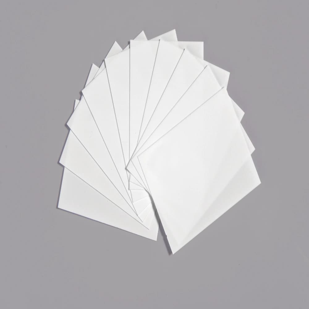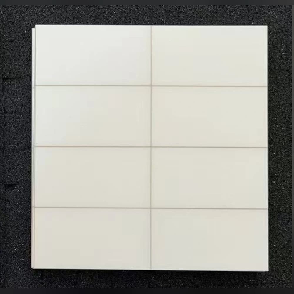
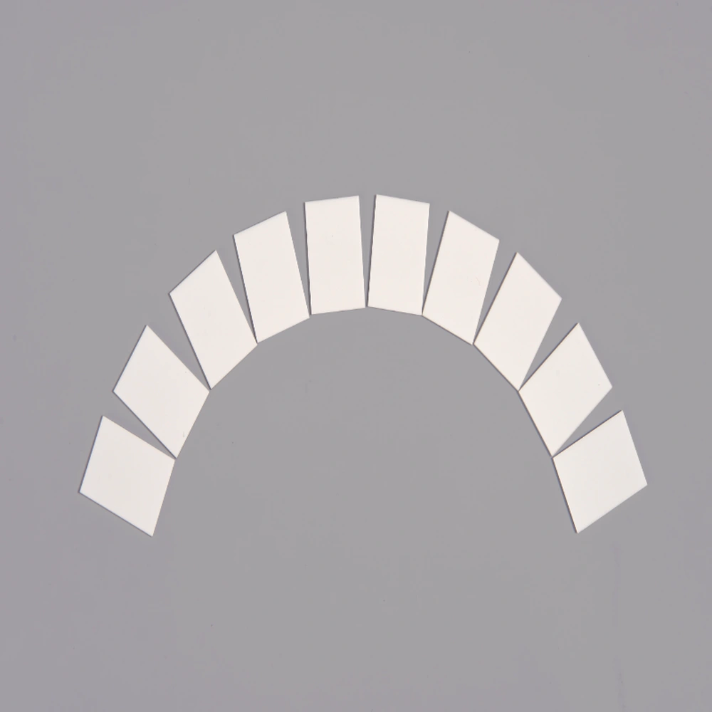
Alumina Substrates for Thin-Film Integrated Circuits
Ceramic Substrate
SKU: FWM/CS-ALU-005
- Material
- Alumina
- Size
- Custom sizes by drawing
- MOQ
- By quotation
- Applications
- Thin-Film Circuits
Surface-controlled alumina substrates for thin-film integrated circuits and precision electronic packaging.
Browse Products
Alumina Ceramic Products
Zirconia Ceramic Products
Silicon Carbide Products
Silicon Nitride Products
Aluminum Nitride Products
Product Description

Alumina substrates provide an electrically insulating carrier for deposited conductors, resistors and other thin-film circuit layers.
A controlled ceramic surface supports fine-pattern definition and film adhesion in microelectronic fabrication. The bare carrier and the deposited circuit are separate supply stages.
A substrate for thin-film processing is not necessarily supplied with a deposited circuit. Confirm surface requirements and the intended film system separately.
Product Advantages
- The insulating surface supports deposited conductors, resistors and other thin-film layers.
- A rigid carrier provides the mechanical base for fine-pattern fabrication.
- Surface preparation connects the ceramic interface to the selected deposition and adhesion system.
Typical Applications
- Thin-Film Circuits: the alumina carrier supports deposited circuit layers.
- Microelectronics: electrically isolated mounting surfaces support compact circuit assemblies.
Technical Data
96% Alumina Substrate (708 S) Properties
| Property | 96% Al₂O₃ — 708 S | Test conditions / measurement tolerance ±10% |
|---|---|---|
| Density (g/cm³) | ≥3.75 | DIN EN 993-1 |
| Bending strength, σ₀ (MPa) | ≥500 | — |
| Young’s modulus (GPa) | ≥300 | — |
| Thermal conductivity (W/(m·K)) | 24 | Room temperature; DIN EN 821-2 |
| Linear thermal expansion coefficient (10⁻⁶/K) | 7–9 | 100–800°C; DIN 51045-1 |
| Specific heat capacity (J/(g·K)) | ≥0.75 | 20°C; DIN EN 821-3 method B |
| Relative permittivity | ~9.8 | Room temperature, 1 MHz; Ra ≤0.4 µm |
| Dielectric loss factor | ≤0.005 | Room temperature; 1 MHz; Ra ≤0.4 µm |
| Volume resistivity (Ω·cm) | ≥10¹⁴ | Room temperature; IEC 62631-3 |
| Breakdown strength (kV/mm) | AC≥15; DC≥15 | 20°C; AC / DC |
| Fracture toughness (MPa·m½) | ≥3.0 | Indentation-fracture (IF) |
How to Read the Parameters
- Purity
Composition identifies a material class, not a guaranteed circuit result.
Specify: Grade designation and relevant property report.
- Surface texture
Ra or Rq describes a defined ceramic surface in µm or nm.
Specify: Functional face, measurement method and local defect criteria.
- Flatness and thickness
Flatness, total thickness variation and parallelism describe different geometry.
Specify: Datums, span, support state and measurement method.
- Electrical properties
Volume resistivity uses Ω·cm or Ω·m; insulation resistance uses Ω.
Specify: Temperature, humidity, voltage, electrification time and specimen geometry.
Alumina: material and surface selection
Alumina is an electrically insulating ceramic platform for printed-film, thin-film and package constructions. Purity, surface condition and geometry must be selected for the downstream process; a bare plate is not a completed circuit.
01Define the grade
Select the alumina formulation and the intended film, metallization or assembly route.
02Form and fire
Ceramic forming and firing establish the body; the chosen route must account for shrinkage and the required finished geometry.
03Finish functional features
Where specified, machine or laser-process features and prepare the functional surfaces.
04Inspect the delivered condition
Assess dimensions, surfaces and edge condition against the drawing before later circuit processing.
Application Conditions & Design Review
Start with the deposition surface
Thin-film fabrication needs a surface specification that addresses texture, defects and cleanliness. Material grade alone does not establish whether a carrier is ready for a particular deposition and patterning process.
Define the complete layer system
Identify adhesion, conductive, resistive and dielectric layers separately. The intended film process and assembly method determine which surface preparation and finish requirements matter most.
Film compatibility
Select the grade and surface for the actual resistor, conductor or deposited-film system, not purity alone.
Functional geometry
Identify circuit areas, datums, mounting features and separation edges.
Thermal and electrical role
Balance ceramic thickness, heat transfer and isolation within the completed assembly.
Send With Your Drawing
- Alumina grade, outline, thickness and designated deposition face.
- Surface roughness, flatness, defect criteria and cleaning restrictions.
- Film-stack materials, patterning route and assembly requirements.
Include the drawing revision, sample and production quantities, and required inspection documents.
Define Acceptance Before Production
- Inspect the functional face against agreed texture, geometry and defect criteria.
- Qualify film adhesion and electrical behavior on the intended film stack.
Agree the test methods, sampling plan, acceptance limits and required reports before production.
Available Forms & Processing
Product-specific geometry and processing features.
- 96% alumina carrier outlines and thicknesses matched to the circuit layout.
- Surface roughness, local defects and cleanliness defined for the deposition interface.
- Bare or separately metallized supply stages identified independently from the functional film stack.
Engineering Questions
Can an as-fired plate be used for every thin-film process?
No single finish suits every process. Review the feature scale and film thickness, then specify the surface condition and validate it with representative deposition trials.
Is higher-purity alumina always the better substrate?
No. The preferred grade depends on film compatibility, surface condition, geometry and assembly needs. Purity alone does not establish resistor stability or thin-film yield.
Does a hole in alumina provide an electrical via?
No. A hole is a geometric feature until a compatible conductor or metallization structure is specified and qualified.
Packaging & Shipping
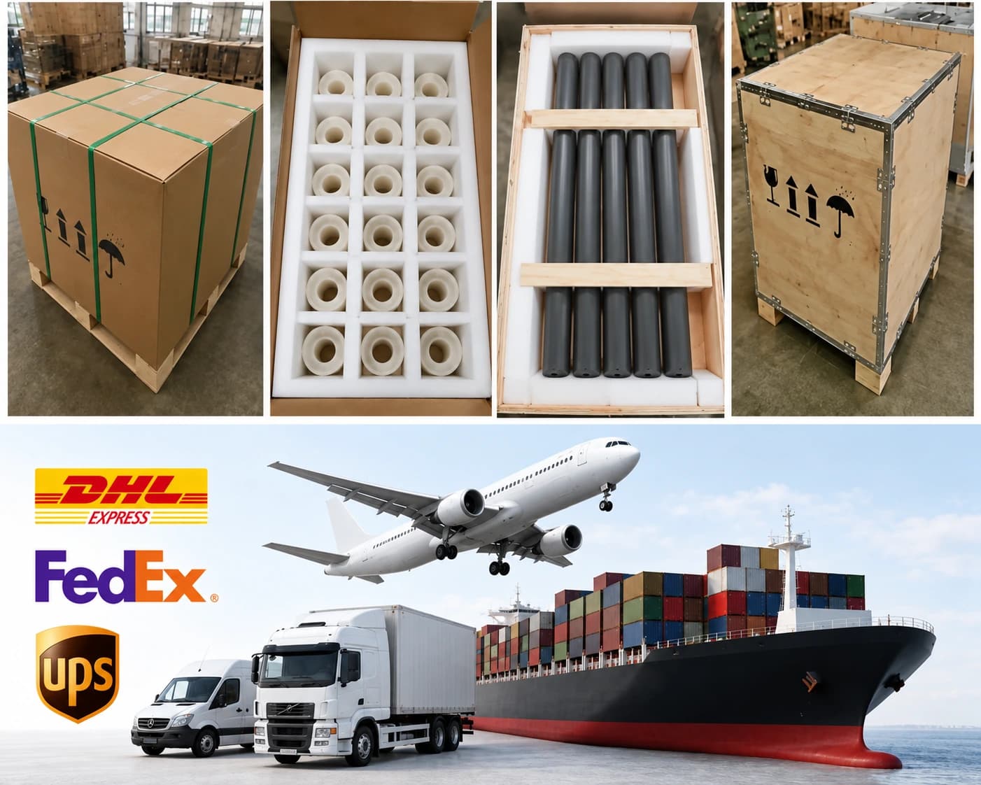
Packaging is selected for substrate finish, quantity and export handling.
| Item | Details |
|---|---|
| Packaging approach | Packaging is selected for substrate finish, quantity and export handling. |
| Protection methods | Individual separation; Anti-scratch interlayers for polished surfaces; Tray or foam protection; Inner box and export carton; Moisture protection where appropriate; Wooden case for larger export consignments when required |
| MOQ reference | By quotation |
| Lead-time references | Quotation inputs: Drawing, material, finish, quantity and delivery destination |
| Payment terms | T/T / Western Union / PayPal; 50% advance payment, 50% balance before shipment |
| Shipping methods | Sea freight / Air freight / Door-to-door courier |
Related Ceramic Substrate Products
Compare related ceramic substrate materials and metallization routes within the same product family.