AlN Ceramic Substrates for Thin-Film Circuits
Ceramic Substrate
SKU: FWM/CS-ALN-004
- Material
- Aluminum Nitride
- Size
- Custom sizes by drawing
- MOQ
- By quotation
- Applications
- Thin-Film Circuits
Surface-controlled AlN substrates for thin-film circuits and compact high-heat-flux electronic packages.
Browse Products
Alumina Ceramic Products
Zirconia Ceramic Products
Silicon Carbide Products
Silicon Nitride Products
Aluminum Nitride Products
Product Description

AlN thin-film substrates are insulating carriers for deposited circuits in compact electronic and optoelectronic packages.
Their heat-conducting ceramic body helps move heat away from concentrated devices, and a controlled surface supports the deposited film stack. Adhesion layers, functional films and bond-pad finishes are part of the circuit construction.
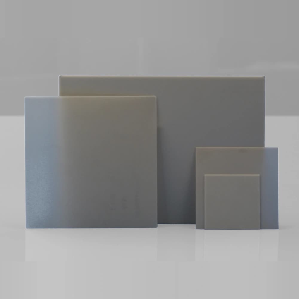
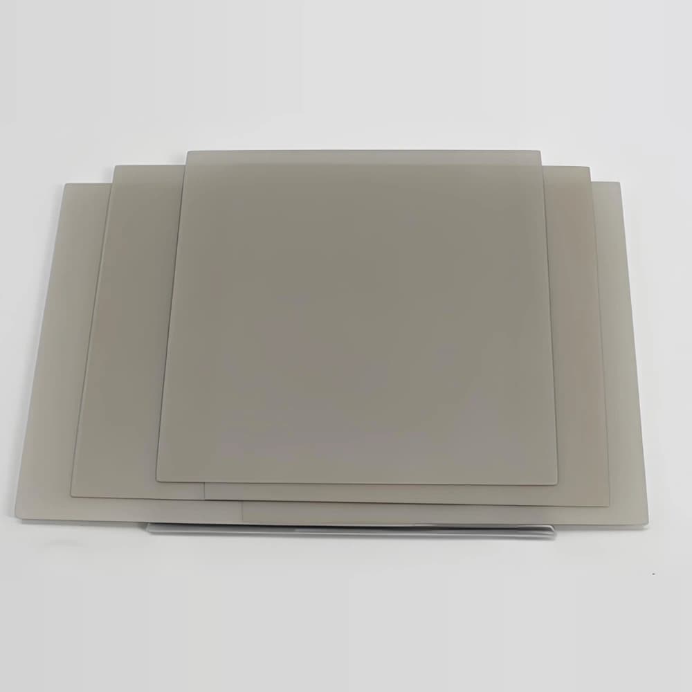
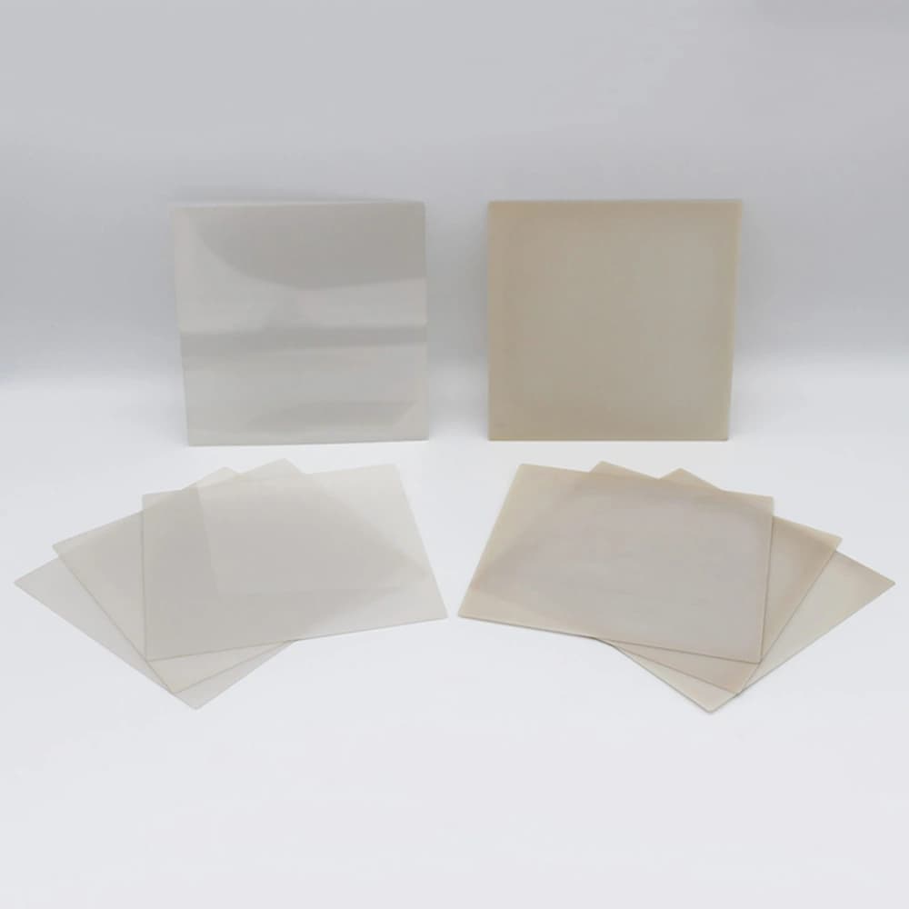
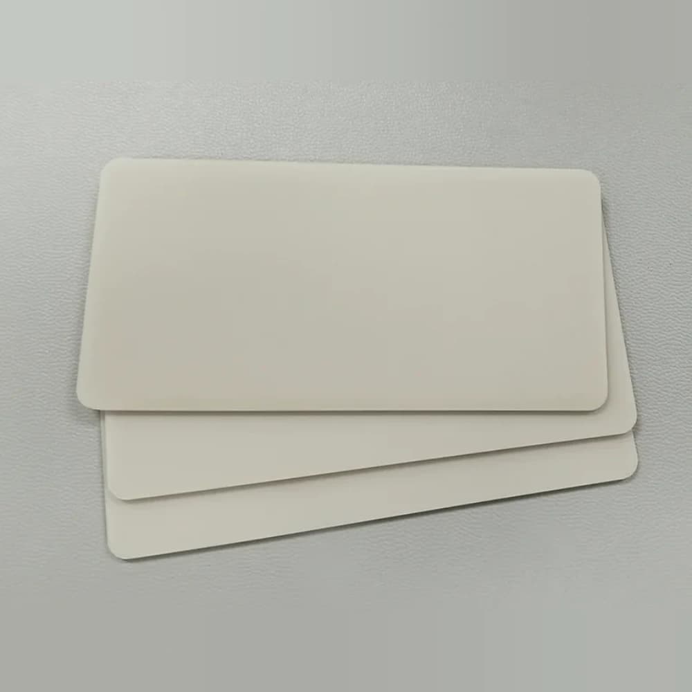
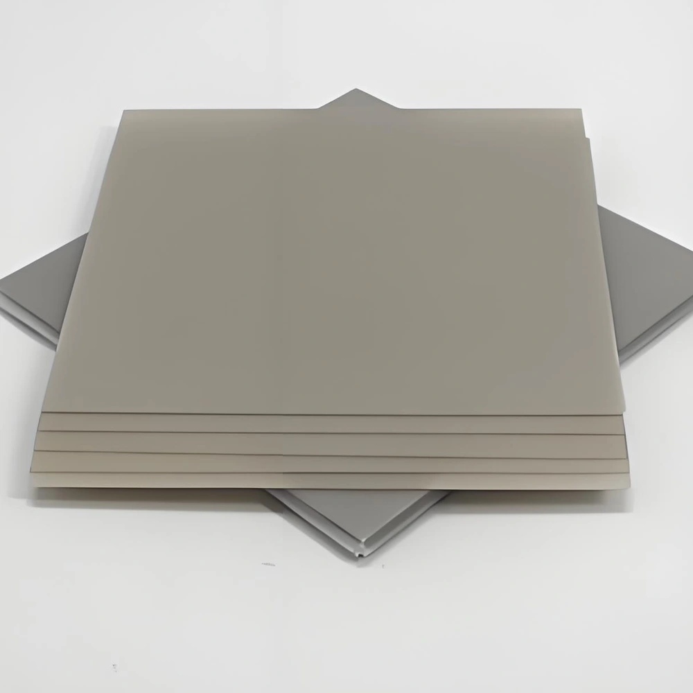
The images illustrate a surface-finished substrate. Specify the required finish on each face; gloss alone does not demonstrate surface roughness or flatness.
Product Advantages
- A controlled AlN surface supports deposited conductors and other functional films.
- The insulating ceramic conducts heat away from concentrated device locations.
- Carrier geometry provides stable attachment and registration interfaces for compact circuits.
Typical Applications
- Thin-Film Circuits: AlN carries the deposited film stack and connection-pad layout.
- High-Heat-Flux Electronics: insulating carriers support compact devices with localized heat generation.
Technical Data
95% AlN Substrate Properties
| Property | 95% AlN typical value | Condition / method |
|---|---|---|
| AlN content (%) | 95 | — |
| Density (g/cm³) | ≥3.3 | — |
| Flexural strength (MPa) | ≥400 | — |
| Thermal conductivity (W/(m·K)) | ≥170 | Room temperature |
| Relative permittivity | 8–10 | 1 MHz; room temperature |
| Dielectric loss tangent | ≤0.0003 | 1 MHz; room temperature |
| Dielectric strength (kV/mm) | 17 | — |
| Volume resistivity (Ω·cm) | ≥10¹⁴ | — |
How to Read the Parameters
- Thermal conductivity
A ceramic property in W/(m·K), not a complete-stack rating.
Specify: Grade, temperature, direction where relevant and method.
- Thermal resistance
A defined heat-path result in K/W.
Specify: Heat-source area, layer dimensions, interfaces and cooling boundary.
- Thermal expansion
CTE is expressed in ppm/K or ×10⁻⁶/K over an interval.
Specify: Temperature interval and whether the value describes ceramic or the effective stack.
- Surface and geometry
A high-conductivity grade does not determine roughness or flatness.
Specify: Functional faces, thickness variation and dimensional acceptance separately.
AlN: an insulating thermal path
Aluminum nitride is considered when ceramic heat transfer is a major constraint. Its bulk conductivity must be distinguished from the thermal resistance of the finished substrate and module.
01Define the thermal requirement
Identify the heat-source footprint, temperature target, cooling interface and intended conductor system.
02Select the AlN grade
Review ceramic conductivity and other material properties at the relevant conditions.
03Prepare the specified form
Choose the delivered bare, machined or surface-finished condition for subsequent processing.
04Validate the interfaces
Evaluate film or metallization compatibility, attachment and cooling interfaces as part of the full construction.
Application Conditions & Design Review
Specify the film interface
An AlN carrier used for thin films needs a defined surface and compatible adhesion-layer system. The base ceramic, deposited layers and final bond pads should be described as separate parts of the design.
Keep thermal and RF requirements distinct
A thermally favorable carrier does not automatically establish RF performance. Define the operating frequency and circuit geometry alongside the thermal load and assembly interfaces.
Heat path
Include ceramic thickness, copper, attachment layers and contact area in the thermal assessment.
Downstream process
Identify deposited films or printed pastes, firing atmosphere and chemical exposures before selecting the surface.
Finished delivery state
Distinguish an as-fired blank from a polished plate or an already metallized substrate.
Send With Your Drawing
- AlN grade, thickness, deposition-face roughness and defect criteria.
- Adhesion/conductor/functional-film stack and patterning requirements.
- Frequency-dependent electrical targets, heat load and attachment process.
Include the drawing revision, sample and production quantities, and required inspection documents.
Define Acceptance Before Production
- Inspect the designated film surface and drawing-defined geometry.
- Qualify adhesion and circuit performance with the actual film stack and test conditions.
Agree the test methods, sampling plan, acceptance limits and required reports before production.
Available Forms & Processing
Product-specific geometry and processing features.
- AlN outlines, thicknesses and registration datums matched to the film layout.
- Surface texture and local defects defined for the deposition and adhesion system.
- Adhesion layers, functional films and pad finishes identified separately from the bare ceramic.
Engineering Questions
Does choosing AlN establish a maximum operating frequency?
No. Frequency performance depends on dielectric behavior, conductor geometry, layer stack and package construction. Validate the complete circuit at the intended frequency.
Does high AlN conductivity guarantee a cooler module?
No. The benefit depends on ceramic thickness, heat-source area, attachment layers and heat rejection. Evaluate the complete heat path.
Can an alumina film process be transferred directly to AlN?
Not without review. Confirm that the paste or deposited stack, atmosphere, thermal cycle and cleaning chemistry are compatible with the selected AlN system.
Packaging & Shipping
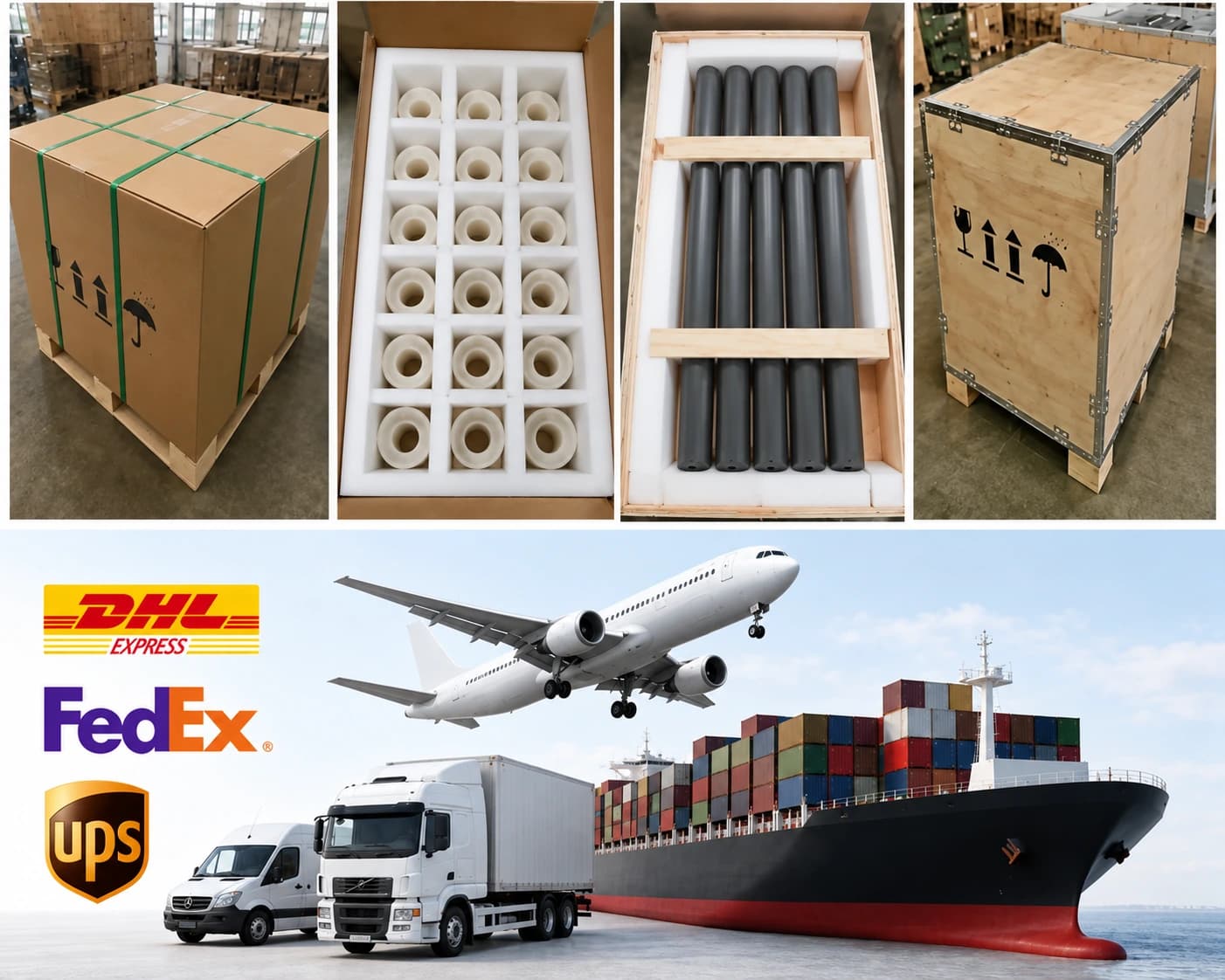
AlN substrates receive individual separation and surface protection appropriate to the finish.
| Item | Details |
|---|---|
| Packaging approach | AlN substrates receive individual separation and surface protection appropriate to the finish. |
| Protection methods | Individual separation; Anti-scratch interlayers; Rigid trays or foam protection; Moisture protection where appropriate; Inner box and export carton; Wooden case when required |
| MOQ reference | By quotation |
| Lead-time references | Quotation inputs: Drawing, material, finish, quantity and delivery destination |
| Payment terms | T/T / Western Union / PayPal; 50% advance payment, 50% balance before shipment |
| Shipping methods | Sea freight / Air freight / Door-to-door courier |
Related Ceramic Substrate Products
Compare related ceramic substrate materials and metallization routes within the same product family.