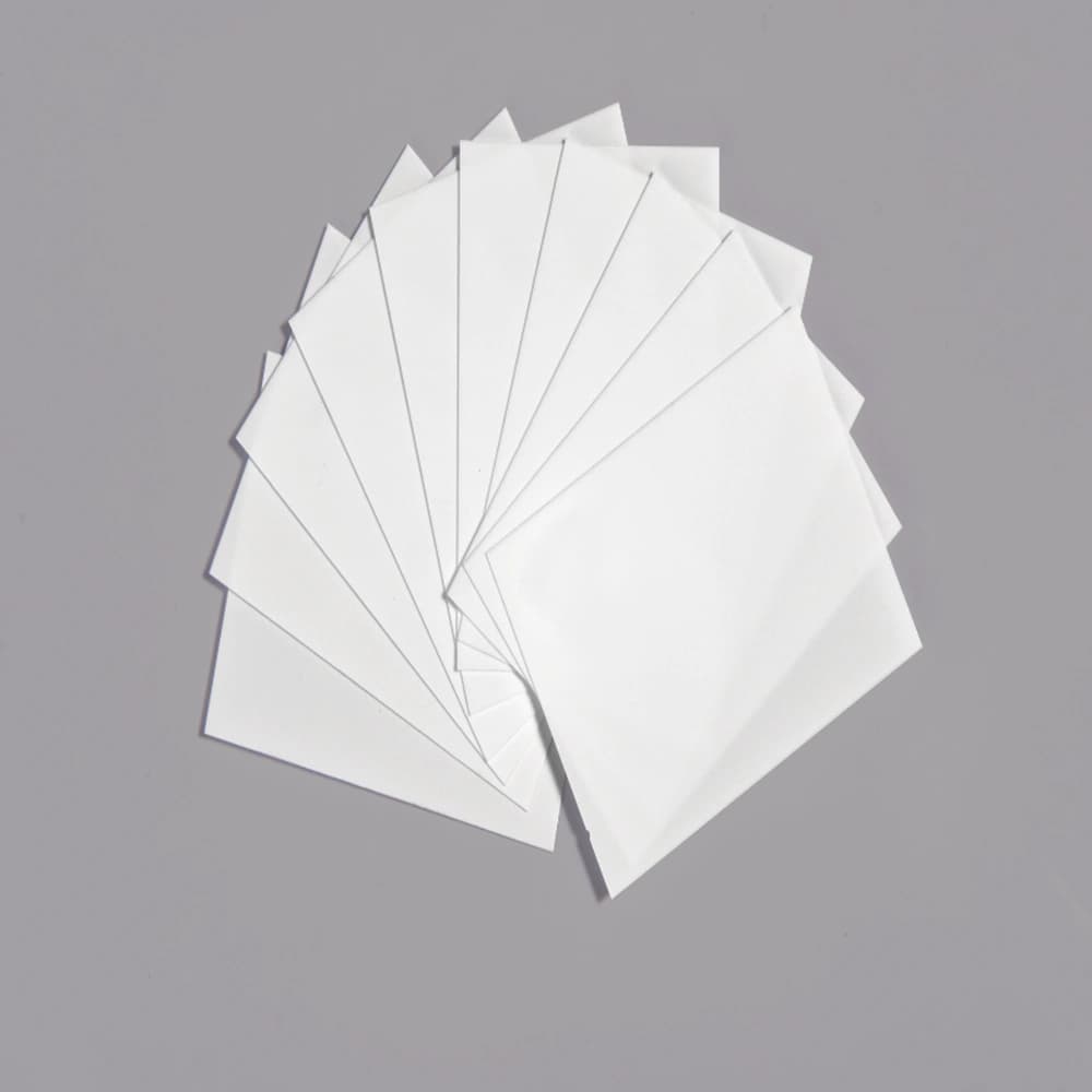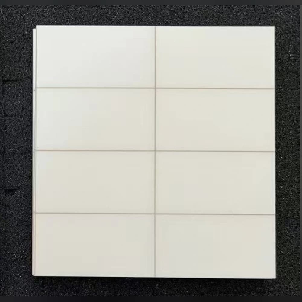
99.6% High-Purity Polished Alumina Ceramic Substrates
Ceramic Substrate
SKU: FWM/CS-ALU-009
- Material
- Alumina
- Size
- Custom sizes by drawing
- MOQ
- By quotation
- Applications
- Thin-Film Circuits
Polished high-purity alumina substrates for thin-film, optical and precision microelectronic processes.
Browse Products
Alumina Ceramic Products
Zirconia Ceramic Products
Silicon Carbide Products
Silicon Nitride Products
Aluminum Nitride Products
Product Description

Polished high-purity alumina substrates provide smooth insulating surfaces for thin-film circuits, die attachment and precision optoelectronic assemblies.
Polishing controls local surface texture for deposition and bonding. Flatness, parallelism and thickness variation describe different geometric requirements.
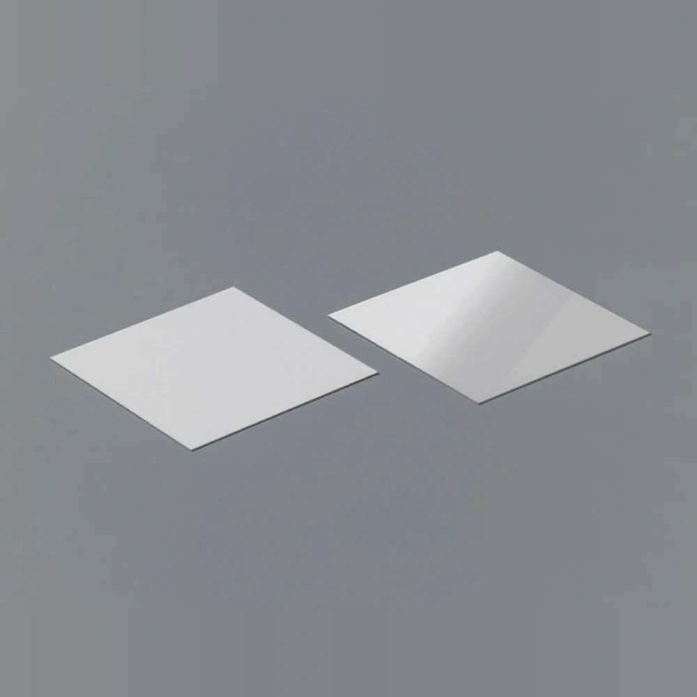
Controlled reflections illustrate the surface finish, not a measured roughness or flatness value. Confirm polished faces and acceptance criteria in the drawing.
Product Advantages
- Polished faces provide controlled local texture for deposition and attachment.
- High-purity alumina supplies an electrically insulating platform for precision circuits.
- The surface and geometric specifications can address different requirements on each face.
Typical Applications
- Thin-Film Circuits: polished ceramic faces support deposition and fine-pattern processing.
- Optoelectronics: insulating mounting surfaces support die attachment and package assembly.
Technical Data
99.6% Alumina Substrate (710 C) Properties
| Property | 99.6% Al₂O₃ — 710 C | Test conditions / measurement tolerance ±10% |
|---|---|---|
| Density (g/cm³) | ≥3.80 | DIN EN 993-1 |
| Bending strength, σ₀ (MPa) | ≥420 | ASTM C1499-08 |
| Young’s modulus (GPa) | ≥300 | — |
| Thermal conductivity (W/(m·K)) | ≥25 | Room temperature; DIN EN 821-2 |
| Linear thermal expansion coefficient (10⁻⁶/K) | 7–9 | 100–800°C; DIN 51045-1 |
| Specific heat capacity (J/(g·K)) | ≥0.65 | 20°C; DIN EN 821-3 method B |
| Relative permittivity | 8.5–11.5 | Room temperature, 1 MHz |
| Dielectric loss factor | ≤0.010 | Room temperature; 1 MHz; Ra ≤0.4 µm |
| Volume resistivity (Ω·cm) | ≥10¹⁴ | Room temperature; IEC 62631-3 |
| Breakdown strength (kV/mm) | AC≥15; DC≥15 | 20°C; AC / DC |
| Fracture toughness (MPa·m½) | ≥3.0 | Indentation-fracture (IF) |
How to Read the Parameters
- Ra or Rq
Surface-texture parameters in µm or nm describe different statistical measures.
Specify: Parameter, instrument method, filtering and measurement area or length.
- Total thickness variation
Variation in thickness is distinct from surface roughness.
Specify: Measurement grid, usable area and finished-thickness definition.
- Flatness or parallelism
Geometric controls address shape or the relationship between faces.
Specify: Datums, supports, span and temperature.
- Surface defects
Average roughness does not describe every pit, scratch or edge defect.
Specify: Defect classes, inspection area and acceptance limits.
Polished surfaces: define what the assembly needs
Polishing changes surface texture, while thickness variation, flatness and parallelism describe different geometry. Specify each functional face and the local defect requirements rather than relying on a single roughness value.
01Identify functional faces
Mark surfaces used for film deposition, optical alignment, attachment or thermal contact.
02Set geometry requirements
Define finished thickness, thickness variation and other required shape controls.
03Specify the surface condition
Choose the relevant texture parameter and acceptable local defects for the downstream process.
04Inspect and protect
Verify the agreed surface and geometric criteria, then protect functional faces during handling and shipment.
Application Conditions & Design Review
Specify more than a mirror appearance
A visually reflective finish is not a measurement. Define roughness, surface defects, flatness and thickness variation independently so the finish can be evaluated consistently.
Protect the functional face
Polished surfaces can be selected for deposition, precision bonding or optical assembly. State which face is functional and how it must be handled between finishing and the next operation.
Film integration
Relate surface texture and defects to the actual film stack and patterning requirements.
One or two faces
State whether both faces are functional and whether their specifications differ.
Attachment interfaces
Surface requirements can differ for die attachment, wire bonding and a thermal interface.
Send With Your Drawing
- Polished face designation, roughness parameter and surface-defect limits.
- Finished thickness, total thickness variation, flatness and measurement datums.
- Subsequent deposition or bonding process and packaging/handling requirements.
Include the drawing revision, sample and production quantities, and required inspection documents.
Define Acceptance Before Production
- Measure specified surface and geometric parameters using agreed methods.
- Inspect functional faces for unacceptable scratches, pits and contamination.
Agree the test methods, sampling plan, acceptance limits and required reports before production.
Available Forms & Processing
Product-specific geometry and processing features.
- 99.6% alumina with the polished face or faces identified on the drawing.
- Surface roughness, flatness, parallelism and total thickness variation specified separately.
- Outlines, edge condition and functional-area defect limits matched to the assembly.
Engineering Questions
Does double-sided polishing guarantee parallel faces?
No. The polishing requirement and the geometric acceptance limits must be stated separately. Specify parallelism or thickness variation when it matters to the assembly.
Does low Ra guarantee a flat substrate?
No. Roughness describes local texture; flatness and thickness variation must be controlled separately.
Should both polished faces have the same specification?
Only if the assembly requires it. Define the function and acceptance criteria of each face separately.
Packaging & Shipping
Packaging is selected for substrate finish, quantity and export handling.
| Item | Details |
|---|---|
| Packaging approach | Packaging is selected for substrate finish, quantity and export handling. |
| Protection methods | Individual separation; Anti-scratch interlayers for polished surfaces; Tray or foam protection; Inner box and export carton; Moisture protection where appropriate; Wooden case for larger export consignments when required |
| MOQ reference | By quotation |
| Lead-time references | Quotation inputs: Drawing, material, finish, quantity and delivery destination |
| Payment terms | T/T / Western Union / PayPal; 50% advance payment, 50% balance before shipment |
| Shipping methods | Sea freight / Air freight / Door-to-door courier |

Related Ceramic Substrate Products
Compare related ceramic substrate materials and metallization routes within the same product family.