AlN AMB Copper-Clad Substrates
Ceramic Substrate
SKU: FWM/CS-AMB-001
- Material
- Aluminum Nitride (AlN) / Copper
- Size
- 240 × 280 mm panel reference; custom layer stack
- MOQ
- Confirmed by quotation
- Applications
- Power Modules · Thermal Management
FreeWill Material supplies aluminum nitride (AlN) AMB copper-clad substrates for power modules that need efficient heat transfer, electrical insulation and drawing-defined copper circuits.
Browse Products
Alumina Ceramic Products
Zirconia Ceramic Products
Silicon Carbide Products
Silicon Nitride Products
Aluminum Nitride Products
Product Description

AlN ceramic insulation and active-metal-brazed copper circuits for power-module thermal management.
An AlN AMB substrate combines an aluminum nitride insulating layer with copper joined by active metal brazing. The copper forms current-carrying paths and attachment surfaces, while the ceramic provides an electrically insulating heat path toward the cooling interface.
Single- or double-sided copper layouts support IGBT and SiC devices in traction inverters, industrial drives and power converters. Ceramic, copper and braze form one construction tailored to the module footprint.
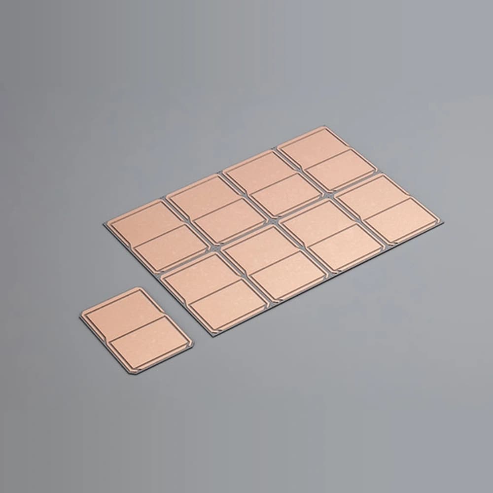
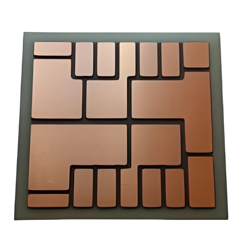
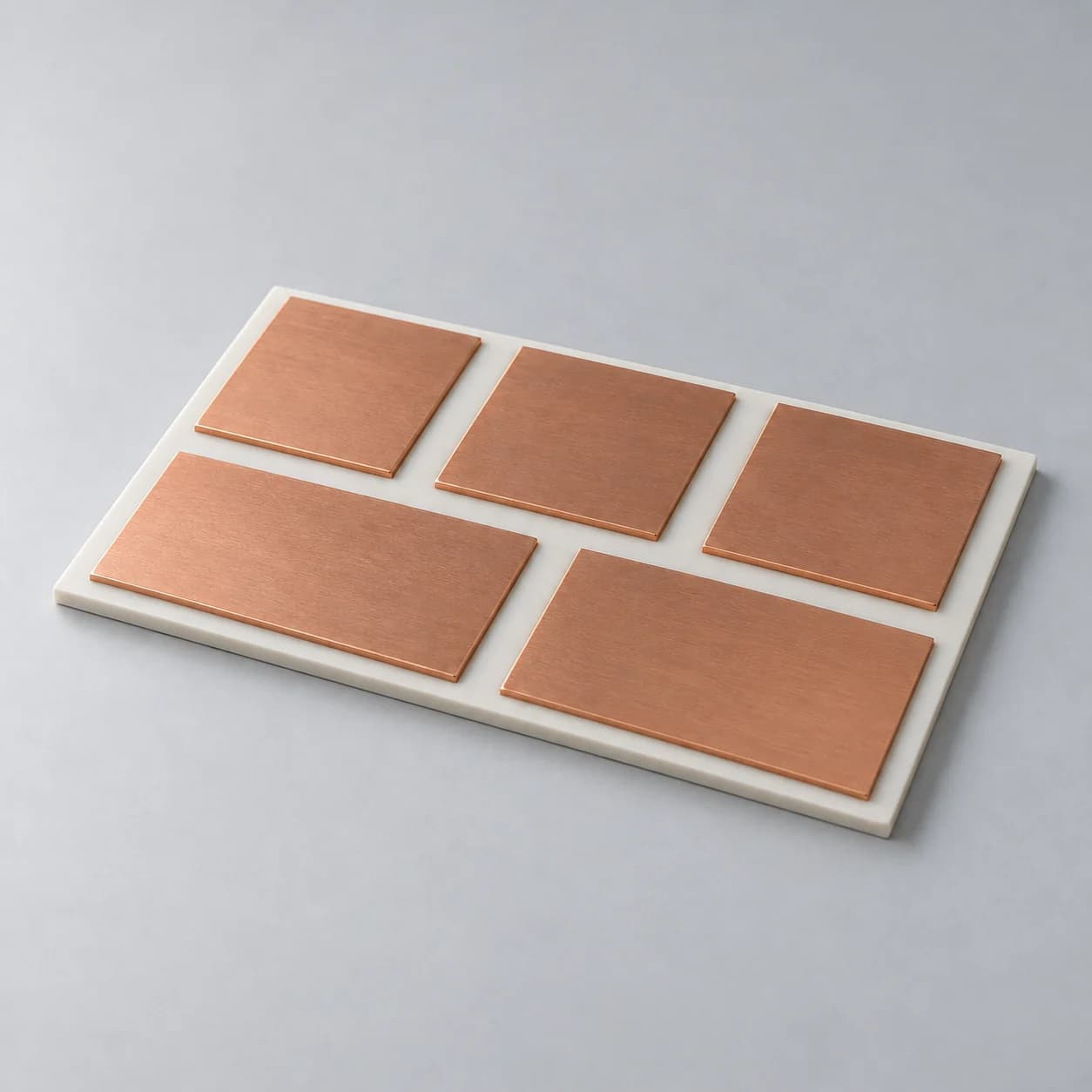
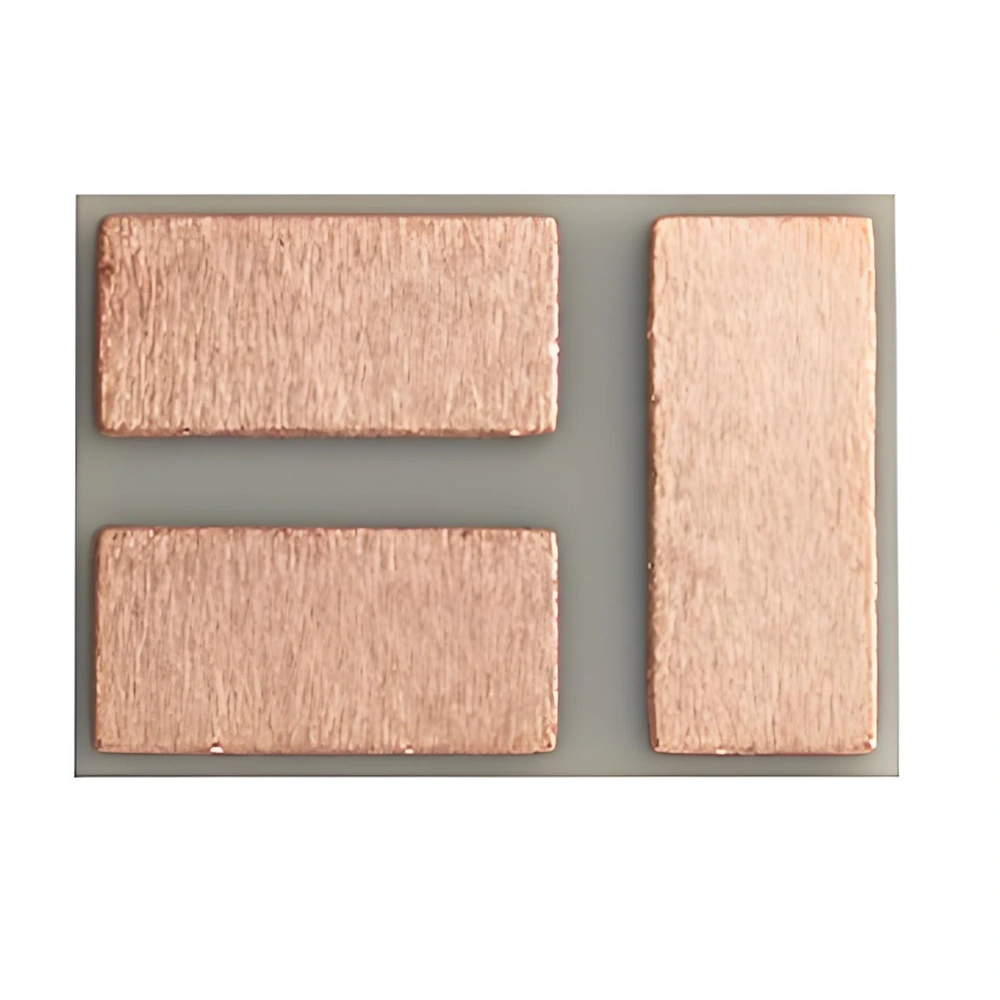
The illustration represents copper on AlN. AMB uses an active-metal braze at the ceramic interface; the process and layer specifications require supplier confirmation.
Product Advantages
- Heat-conducting ceramic: the AlN layer transfers heat away from power devices while maintaining electrical separation from the cooling structure.
- Integrated copper circuits: bonded copper provides current-carrying paths and spreads heat across the ceramic surface.
- Active-metal-brazed interface: the braze joins copper to AlN as a copper-clad substrate rather than a loose stack of separate layers.
- Electrical insulation: the ceramic separates electrically live conductors from adjacent surfaces; the complete circuit geometry determines module insulation performance.
- Assembly surfaces: patterned copper and specified finishes provide attachment areas for semiconductor dies and interconnections.
- Configurable layout: single- or double-sided copper patterns combine current paths, device footprints and heat-spreading areas within the substrate outline.
Typical Applications
- EV and HEV power conversion: candidate substrates for traction inverters, on-board chargers and DC-DC converters using IGBT or SiC devices, subject to module reliability and automotive qualification requirements.
- Renewable energy and grid equipment: power-module packaging for solar and wind inverters, energy-storage converters and selected high-voltage conversion systems, with insulation and thermal performance reviewed at module level.
- Industrial motor drives and UPS: electrically insulated power circuits for variable-speed drives, robotics and uninterruptible power supplies requiring controlled heat transfer during continuous operation.
- Advanced power semiconductor packaging: custom copper layouts for IGBT and SiC modules where ceramic grade, die attachment, interconnection and cooling interfaces are developed as one thermal and electrical system.
Technical Data
Typical Construction Parameters
| Parameter | Typical value / configuration | Applicable condition |
|---|---|---|
| Ceramic base | High-purity aluminum nitride (AlN) | Grade and material data sheet |
| Copper layer | Oxygen-free high-conductivity copper | Copper grade and supply condition |
| Bonding route | Active metal brazing (AMB) | Braze system and process route |
| Thermal conductivity | 170–200 W/(m·K) | Selected AlN grade and test method |
| Bond strength | >70 MPa | — |
| Dielectric strength | >15 kV/mm | Thickness, voltage and test conditions |
| Coefficient of thermal expansion | 4.7 × 10⁻⁶/K | Temperature range and assembly design |
| Ceramic thickness | 0.2–2.0 mm | Drawing-defined thickness and tolerance |
| Copper thickness | 0.1–0.6 mm; customizable | Top and bottom copper configuration |
| Maximum panel size | 240 × 280 mm | Usable area, outline and flatness |
| Surface finishes | Immersion gold, OSP, Ni/Au, Ni/Pd, Ag | Finish stack and assembly compatibility |
| Thermal cycling | >5,000 cycles (−55°C to 150°C) | Cycle profile and failure criteria |
How to Read the Parameters
- Bond strength
Peel force per width in N/mm differs from bond stress in MPa.
Specify: Test mode, fixture, specimen, rate and failure location.
- Thermal conductivity
A stated ceramic value is not an effective AMB-stack conductivity.
Specify: Ceramic grade, temperature and method.
- Thermal cycling
A cycle count applies only to its defined construction and profile.
Specify: Endpoints, dwell, ramp/transfer, samples, inspection and failure criteria.
- Layer and panel dimensions
Available combinations cannot be inferred from separate maximum values.
Specify: Complete stack, usable circuit area, outline and finished shape.
AMB: ceramic, braze and copper as one construction
AMB joins copper and ceramic through an active braze system whose reactive elements enable bonding at the ceramic interface. Ceramic grade, braze and copper geometry must be assessed together; generic AMB principles do not establish any one product’s numerical capability.

Application Conditions & Design Review
Use the whole stack in the thermal review
AlN AMB combines a heat-transfer ceramic with copper and a braze interface. Evaluate the complete construction, including attachment layers and cooling, rather than assigning the ceramic conductivity to the finished module.
Review copper and braze together
Top and bottom copper coverage, ceramic thickness and interface design should be coordinated around the intended assembly and duty cycle. Compare reference data only when the stack construction and test conditions are appropriate to the design.
Ceramic choice
Si3N4, AlN and selected alumina configurations address different thermal and mechanical priorities.
Copper distribution
Layer thickness and copper coverage influence current paths, heat spreading and thermomechanical stress.
Mission profile
Define operating temperatures and loading before choosing substrate and assembly qualification tests.
Send With Your Drawing
- AlN grade, ceramic thickness and top/bottom copper thickness and pattern.
- Braze-system requirements, surface finish and device/cooling attachment methods.
- Heat-source map, isolation conditions and qualification profile.
Include the drawing revision, sample and production quantities, and required inspection documents.
Define Acceptance Before Production
- Inspect copper geometry, substrate shape and agreed interface-integrity criteria.
- Define bond and insulation tests with methods and qualify the intended assembly under its duty cycle.
Agree the test methods, sampling plan, acceptance limits and required reports before production.
Available Forms & Processing
Product-specific geometry, copper patterns and attachment interfaces complement the layer dimensions in the technical table.
- Outlines and cut-outs: usable area, flatness and mounting features defined on the substrate drawing.
- Layer stack: selected AlN grade, active-metal braze and top/bottom copper arrangement identified as one construction.
- Circuit patterns: single- or double-sided current paths, isolation gaps and device footprints coordinated with copper thickness.
- Surface finish: the selected finish stack matched to die attachment, interconnection and storage requirements.
- Production documentation: drawing revision, sample and production quantities, inspection records and protective packing identified for the order.
Engineering Questions
Can Si3N4 AMB reliability data be applied directly to AlN AMB?
No. The ceramic, braze, copper layout and test construction differ. Use data for the specified AlN AMB stack and confirm the relevant test conditions.
Is the active braze the same as component-attach solder?
No. The active braze is part of the ceramic-to-copper joining system. Die-attach solder or sinter material belongs to a later assembly interface.
Can one AMB product’s cycle result be used for another stack?
Not without evidence. Ceramic grade, braze, copper geometry, layer thicknesses and the test profile must be comparable.
How should AlN AMB and Si3N4 AMB substrates be compared?
AlN is a candidate when ceramic heat conduction is a priority. Si3N4 is often considered when fracture toughness and demanding thermal cycling are central. Compare the complete layer stack, copper layout and qualification results for the intended module.
Can the substrate dimensions and layer stack be customized?
Custom layer stacks can be reviewed. Typical construction dimensions include ceramic thickness of 0.2–2.0 mm, copper thickness of 0.1–0.6 mm and a maximum panel size of 240 × 280 mm; these do not establish that every combination is manufacturable. The usable panel area, outline, copper balance and tolerances determine the selected construction.
What information is needed for an AlN AMB quotation?
Send the circuit drawing or Gerber/DXF file, outline and tolerances, ceramic and copper thicknesses, required finish, voltage and thermal conditions, assembly process, quantity and inspection or compliance documents required.
Packaging & Shipping
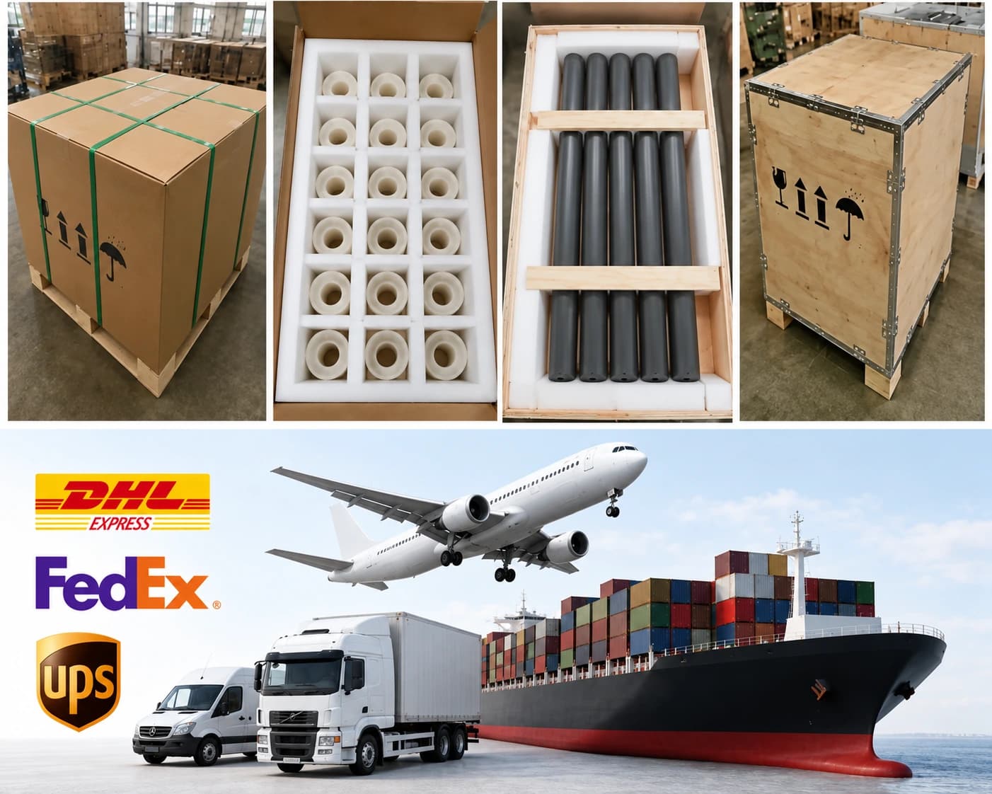
Protective packaging is agreed for the ceramic outline, copper pattern and surface finish to limit handling damage and contamination during international shipment.
| Item | Details |
|---|---|
| Product protection | Individual separation, rigid support and cushioning suited to the approved substrate geometry |
| Surface protection | Clean handling and moisture or oxidation protection agreed for the specified finish |
| Traceability | Part number, drawing revision, batch identification and agreed inspection documents |
| MOQ and lead time | Confirmed after drawing, process, quantity and qualification review |
| Payment terms | T/T / Western Union / PayPal; 50% advance payment, 50% balance before shipment |
| Shipping methods | Sea freight / Air freight / Door-to-door courier |
Related Ceramic Substrate Products
Compare related ceramic substrate materials and metallization routes within the same product family.