Si3N4 AMB Substrates for SiC Power Modules
Ceramic Substrate
SKU: FWM/CS-AMB-002
- Material
- Ceramic / Copper AMB System
- Size
- Custom sizes by drawing
- MOQ
- 5 pieces or one master-card equivalent
- Applications
- SiC Power Modules
Si3N4 AMB substrates for SiC power modules requiring high mechanical reliability and severe thermal cycling.
Browse Products
Alumina Ceramic Products
Zirconia Ceramic Products
Silicon Carbide Products
Silicon Nitride Products
Aluminum Nitride Products
Product Description

These AMB substrates combine a silicon nitride insulating layer with active-metal-brazed copper circuits for silicon carbide power devices.
The copper carries current and spreads heat; the Si3N4 supports the conductors and resists mechanical stress within the joined structure. SiC refers to the semiconductor devices here, not the substrate ceramic.
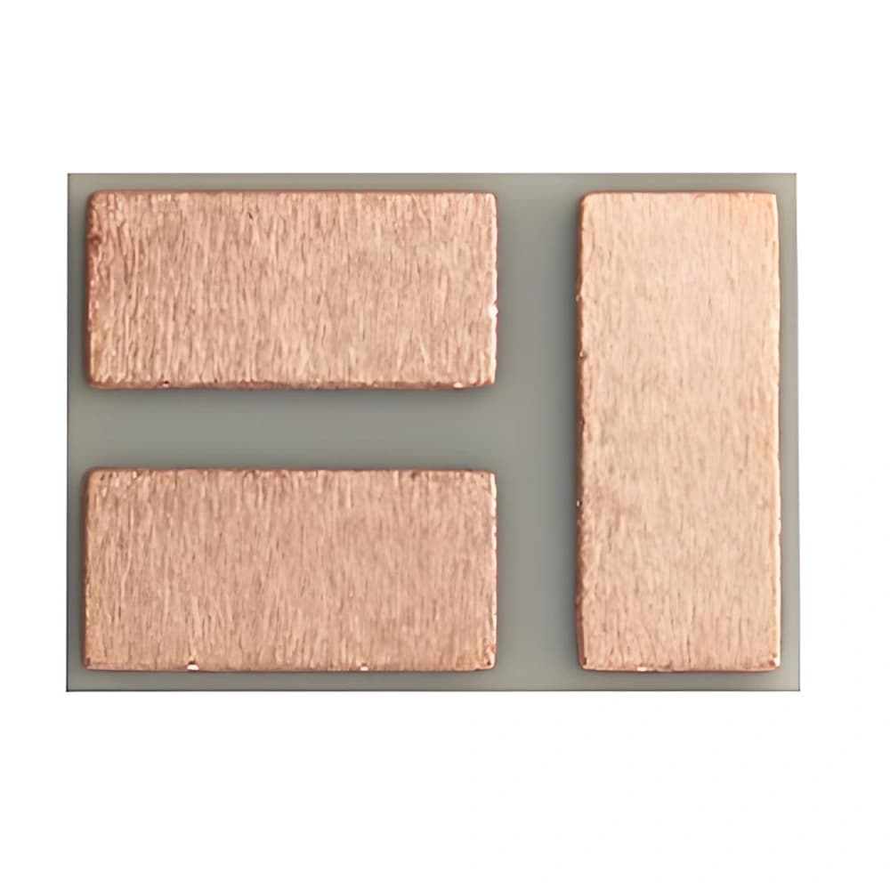
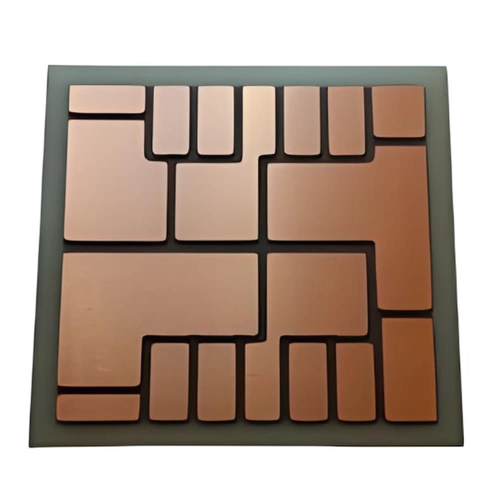
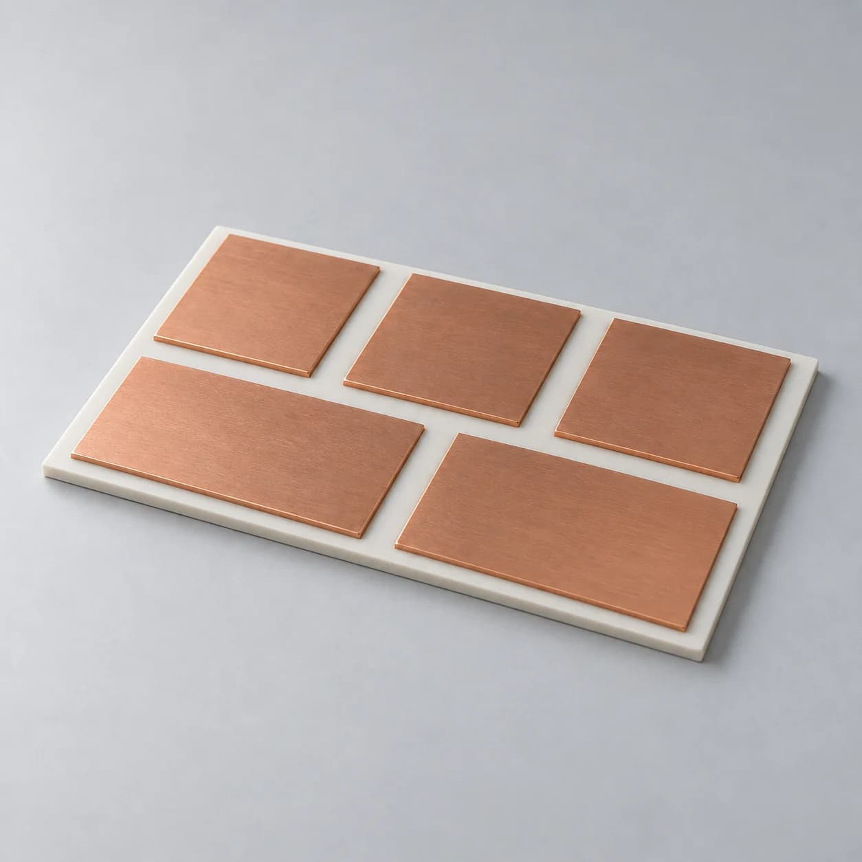
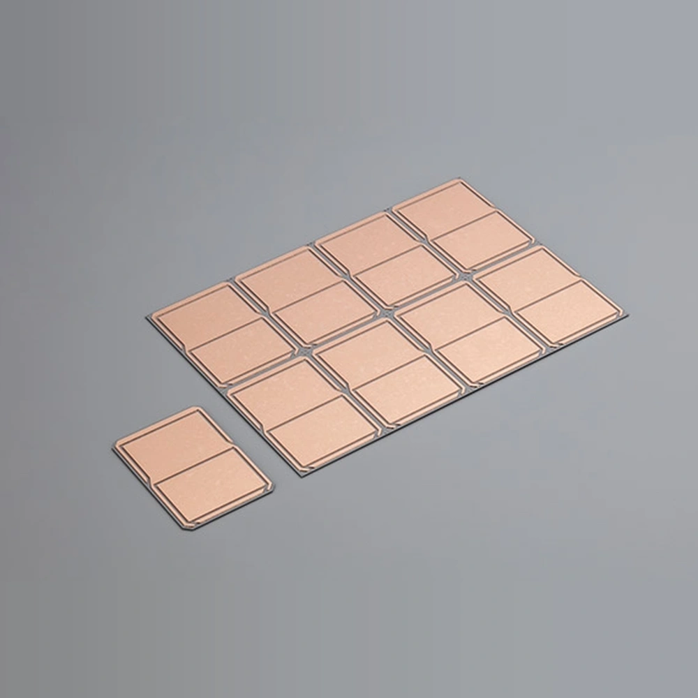
The illustration represents copper on Si3N4. AMB construction, copper thickness and thermal-cycling acceptance are confirmed for the selected design.
Product Advantages
- Copper circuit areas connect SiC devices while spreading heat across the substrate.
- The Si3N4 layer combines electrical isolation with resistance to thermomechanical stress.
- Active-metal-brazed interfaces integrate device-side conductors and the ceramic heat path.
Typical Applications
- SiC Power Modules: Si3N4 AMB carriers support silicon-carbide semiconductor devices.
- EV Traction Inverters: patterned copper provides device-attachment areas and current paths in the module.
Technical Data
Si₃N₄ Substrate (Sinalit) Properties
| Property | Sinalit — bare Si₃N₄ substrate | Conditions / ±10% measurement tolerance (except ref.) |
|---|---|---|
| Density (g/cm³) | ≥3.22 | DIN EN 993-1 |
| Bending strength (MPa) | ≥700 | — |
| Fracture toughness (MPa·m½) | ≥6.5 | Indentation-fracture method |
| Thermal conductivity (W/(m·K)) | 90 | Room temperature; DIN EN 821-2 |
| Coefficient of thermal expansion (10⁻⁶/K) | 3.3 (ref.) | 100–800°C; DIN 51045-1 |
| Dielectric strength (kV/mm) | ≥25 | 20°C; AC / DC; DIN EN 60243-1 |
| Volume resistivity (Ω·cm) | ≥10¹⁴ | Room temperature; IEC 62631-3 |
| Young’s modulus (GPa) | ≥280 | ASTM C1259-15 |
| Specific heat capacity (J/(g·K)) | ≥0.68 | 25°C; DIN EN 821-3 Method B |
| Relative permittivity | 7.8 (ref.) | Room temperature; 1 MHz; Ra ≤0.4 µm; ASTM D150 |
| Dielectric loss tangent | ≤0.003 | Room temperature; 1 MHz; Ra ≤0.4 µm; ASTM D150 |
Typical Construction Parameters
| Construction item | Typical configuration | Applicable condition |
|---|---|---|
| Ceramic base | Silicon nitride (Si3N4) | Grade and route dependent |
| Si3N4 thickness | 0.25 / 0.32 mm | Si₃N₄ ceramic layer |
| Copper thickness | 0.30 / 0.40 / 0.50 / 0.80 mm | Selected AMB layer combinations |
| Pattern | Custom power circuit | Drawing review required |
| Surface finish | Bare Cu and selected plated finishes | Assembly-process dependent |
How to Read the Parameters
- Bond strength
Peel force per width in N/mm differs from bond stress in MPa.
Specify: Test mode, fixture, specimen, rate and failure location.
- Thermal conductivity
A stated ceramic value is not an effective AMB-stack conductivity.
Specify: Ceramic grade, temperature and method.
- Thermal cycling
A cycle count applies only to its defined construction and profile.
Specify: Endpoints, dwell, ramp/transfer, samples, inspection and failure criteria.
- Layer and panel dimensions
Available combinations cannot be inferred from separate maximum values.
Specify: Complete stack, usable circuit area, outline and finished shape.
AMB: ceramic, braze and copper as one construction
AMB joins copper and ceramic through an active braze system whose reactive elements enable bonding at the ceramic interface. Ceramic grade, braze and copper geometry must be assessed together; generic AMB principles do not establish any one product’s numerical capability.

Application Conditions & Design Review
Design around the SiC module
For SiC power modules, review the heat-source footprint and the current/interconnect layout alongside mechanical reliability. Si3N4 is a candidate where strength and fracture resistance are important selection factors.
Define the reliability test article
The substrate, attached dies and completed module represent different qualification stages. Specify which construction is tested and the loading profile instead of using an unqualified cycle count.
Ceramic choice
Si3N4, AlN and selected alumina configurations address different thermal and mechanical priorities.
Copper distribution
Layer thickness and copper coverage influence current paths, heat spreading and thermomechanical stress.
Mission profile
Define operating temperatures and loading before choosing substrate and assembly qualification tests.
Send With Your Drawing
- Si3N4 grade, ceramic/copper thicknesses and top/bottom circuit layout.
- SiC die layout, die-attach and interconnect method, finish and cooling interface.
- Voltage/isolation requirements and thermal/power-cycling conditions.
Include the drawing revision, sample and production quantities, and required inspection documents.
Define Acceptance Before Production
- Inspect circuit geometry, edge condition and agreed braze/interface criteria.
- Validate isolation and cycling behavior on the defined test assembly with stated failure criteria.
Agree the test methods, sampling plan, acceptance limits and required reports before production.
Available Forms & Processing
Product-specific geometry and processing features.
- Si3N4 ceramic with specified copper thicknesses, braze system and circuit pattern.
- Device footprints, current paths, isolation gaps and copper balance defined as one layout.
- Module attachment and cooling interfaces considered separately from substrate thermal-cycle testing.
Engineering Questions
Does choosing Si3N4 AMB automatically qualify a SiC module?
No. It is a substrate selection, not a completed-module qualification. Device attachment, interconnects, cooling and operating conditions must also be validated.
Is the active braze the same as component-attach solder?
No. The active braze is part of the ceramic-to-copper joining system. Die-attach solder or sinter material belongs to a later assembly interface.
Can one AMB product’s cycle result be used for another stack?
Not without evidence. Ceramic grade, braze, copper geometry, layer thicknesses and the test profile must be comparable.
Packaging & Shipping
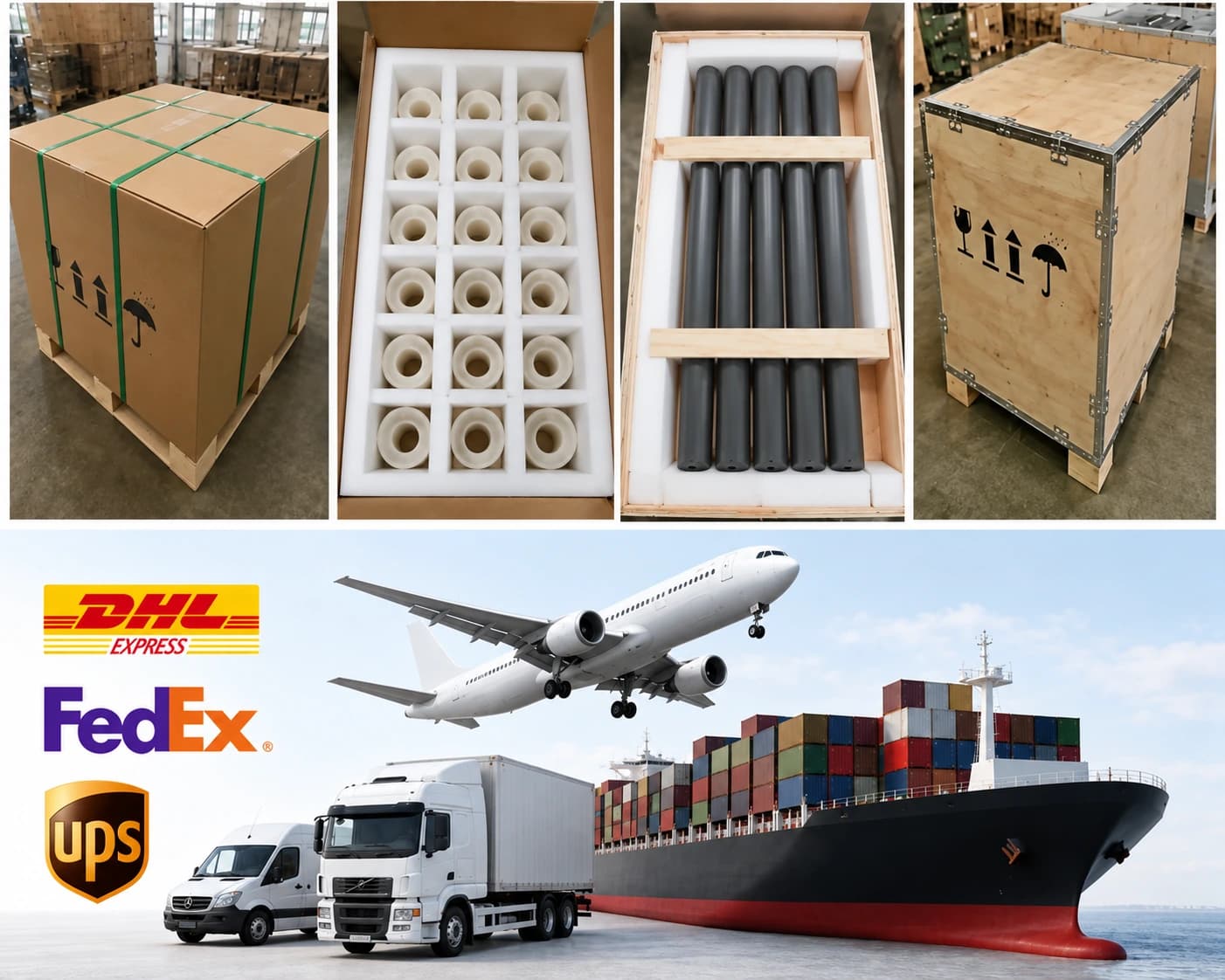
Packaging is selected for master cards, individual units and copper surface condition.
| Item | Details |
|---|---|
| Packaging approach | Packaging is selected for master cards, individual units and copper surface condition. |
| Protection methods | Individual separation; Anti-scratch surface protection; Rigid trays or master-card frames; Copper corrosion protection where appropriate; Inner box and export carton; Wooden case when required |
| MOQ reference | 5 pieces or one master-card equivalent |
| Lead-time references | AMB: 6-10 weeks |
| Payment terms | T/T / Western Union / PayPal; 50% advance payment, 50% balance before shipment |
| Shipping methods | Sea freight / Air freight / Door-to-door courier |
Related Ceramic Substrate Products
Compare related ceramic substrate materials and metallization routes within the same product family.