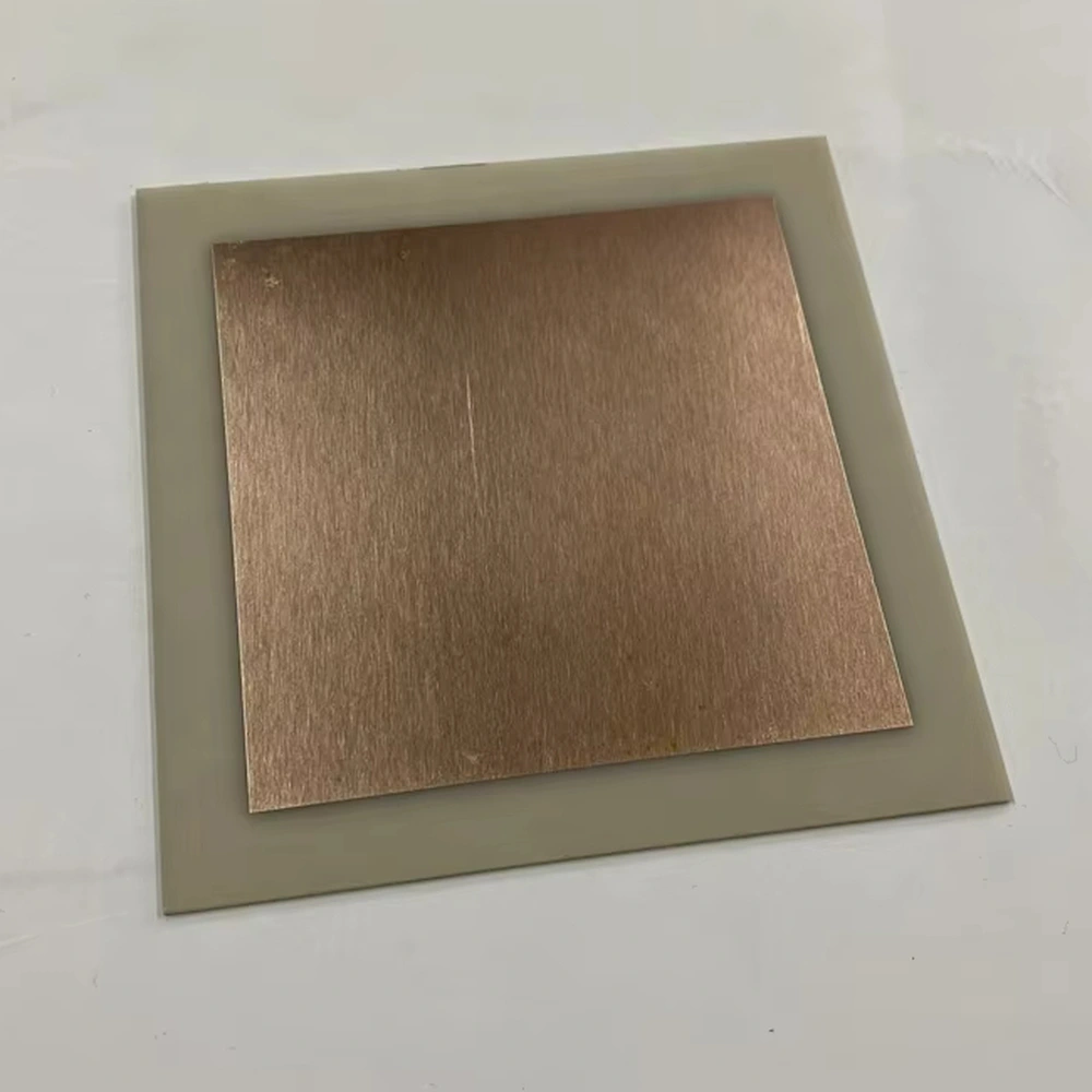
AlN Direct-Bonded Copper DBC Substrates
Ceramic Substrate
SKU: FWM/CS-DBC-004
- Material
- Ceramic / Direct-Bonded Copper System
- Size
- Custom sizes by drawing
- MOQ
- 5 pieces or one master-card equivalent
- Applications
- IGBT Modules
AlN DBC substrates for high-current circuits where bulk heat transfer and electrical insulation are primary constraints.
Browse Products
Alumina Ceramic Products
Zirconia Ceramic Products
Silicon Carbide Products
Silicon Nitride Products
Aluminum Nitride Products
Product Description

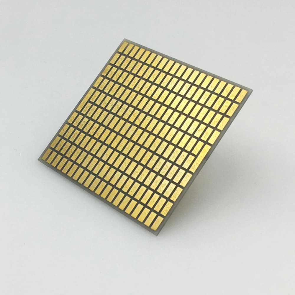
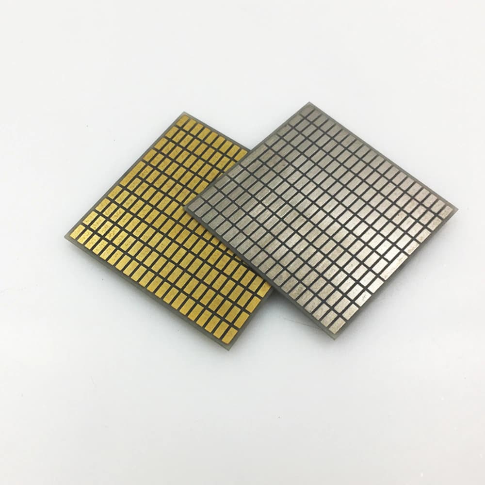
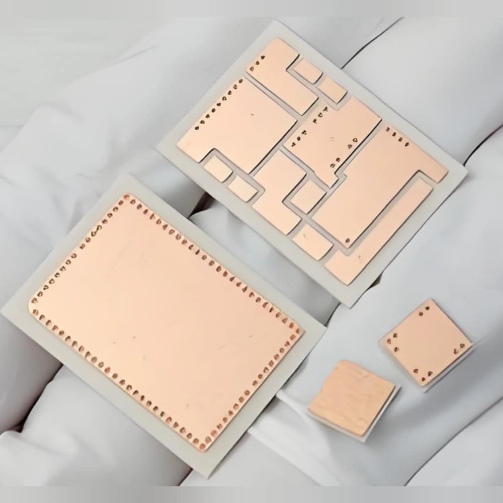
AlN DBC substrates combine bonded copper circuit layers with an aluminum nitride ceramic insulator for power modules and inverters.
The copper supplies electrical paths and device-attachment areas, while the AlN carries heat toward the cooling structure. Thermal resistance depends on the layer thicknesses and bonded interfaces, not ceramic conductivity alone.
Copper bonded to AlN is shown as a reference form. DBC process details, copper layers and acceptance criteria are confirmed with the selected supplier.
Product Advantages
- Copper foil provides power-current paths and device-attachment areas.
- AlN electrically isolates the circuit while conducting heat toward the cooling interface.
- The bonded stack integrates conductors and ceramic support within one circuit carrier.
Typical Applications
- IGBT Modules: bonded copper supports semiconductor attachment over AlN insulation.
- Power Inverters: the ceramic/copper carrier connects current paths with the module heat-removal structure.
Technical Data
95% AlN Substrate Properties
| Property | 95% AlN typical value | Condition / method |
|---|---|---|
| AlN content (%) | 95 | — |
| Density (g/cm³) | ≥3.3 | — |
| Flexural strength (MPa) | ≥400 | — |
| Thermal conductivity (W/(m·K)) | ≥170 | Room temperature |
| Relative permittivity | 8–10 | 1 MHz; room temperature |
| Dielectric loss tangent | ≤0.0003 | 1 MHz; room temperature |
| Dielectric strength (kV/mm) | 17 | — |
| Volume resistivity (Ω·cm) | ≥10¹⁴ | — |
Typical Construction Parameters
| Construction item | Typical configuration | Applicable condition |
|---|---|---|
| Ceramic base | Aluminum nitride (AlN) | Route dependent |
| Ceramic thickness | AlN: 0.25–1.50 mm | Matched ceramic / copper stack |
| Copper thickness | 0.10–0.30 mm | Copper thickness and ceramic stack selected together |
| Line / space | Etched-pattern dependent | Copper thickness, etch profile and insulation clearance |
| Surface finish | Bare/protected Cu; selected Ni, Ni/Au or Ag | Assembly-process dependent |
| Bond / peel testing | Construction-specific test | Peel method, coupon geometry and acceptance criterion |
How to Read the Parameters
- Copper thickness
Foil thickness influences conductor cross-section and etched geometry.
Specify: Finished thickness, sidewall/gap requirements and patterning rules.
- Ceramic conductivity
W/(m·K) describes the ceramic at stated conditions.
Specify: Grade and temperature; keep separate from finished thermal resistance.
- Flatness and copper balance
Incoming ceramic shape does not establish the finished bonded shape.
Specify: Top/bottom pattern, copper-free perimeter and inspection condition.
- Dielectric performance
Material breakdown strength in kV/mm is not an assembly working-voltage rating.
Specify: Stack, gaps, edge clearances, waveform and test conditions.
DBC: bonded copper foil for power circuits
DBC uses a copper–oxygen eutectic interfacial reaction at elevated temperature to join copper foil to a ceramic surface. Conventional AlN DBC includes controlled oxide-surface preparation because AlN is a non-oxide ceramic. The bonded foil is then patterned; it is distinct from printed and fired thick-film conductors or resistors.

Application Conditions & Design Review
Use AlN where the thermal design benefits
AlN DBC combines bonded copper with an insulating ceramic selected for heat transfer. The benefit must be evaluated using the real source area, layer thicknesses and cooling interface.
Include both joining and assembly requirements
Define the copper pattern and the surface needed by die attachment or interconnection. Ceramic conductivity alone does not establish bond integrity, solderability or operating temperature for the completed stack.
Current and geometry
Choose copper thickness with conductor width, spacing and patterning feasibility.
Thermal and mechanical balance
Review ceramic thickness, copper distribution and the completed heat path together.
Hybrid integration
If printed films are needed, define their function and compatibility separately from the bonded copper.
Send With Your Drawing
- AlN grade, ceramic/copper thicknesses and top/bottom layout.
- Finish and die-attach/interconnect/cooling requirements.
- Heat load, operating voltage and defined acceptance/qualification conditions.
Include the drawing revision, sample and production quantities, and required inspection documents.
Define Acceptance Before Production
- Inspect pattern dimensions, substrate shape and specified copper/ceramic interface criteria.
- Define isolation and bond tests, and validate assembly-temperature and thermal performance limits.
Agree the test methods, sampling plan, acceptance limits and required reports before production.
Available Forms & Processing
Product-specific geometry and processing features.
- AlN ceramic thickness and copper thickness selected for the specified bonded stack.
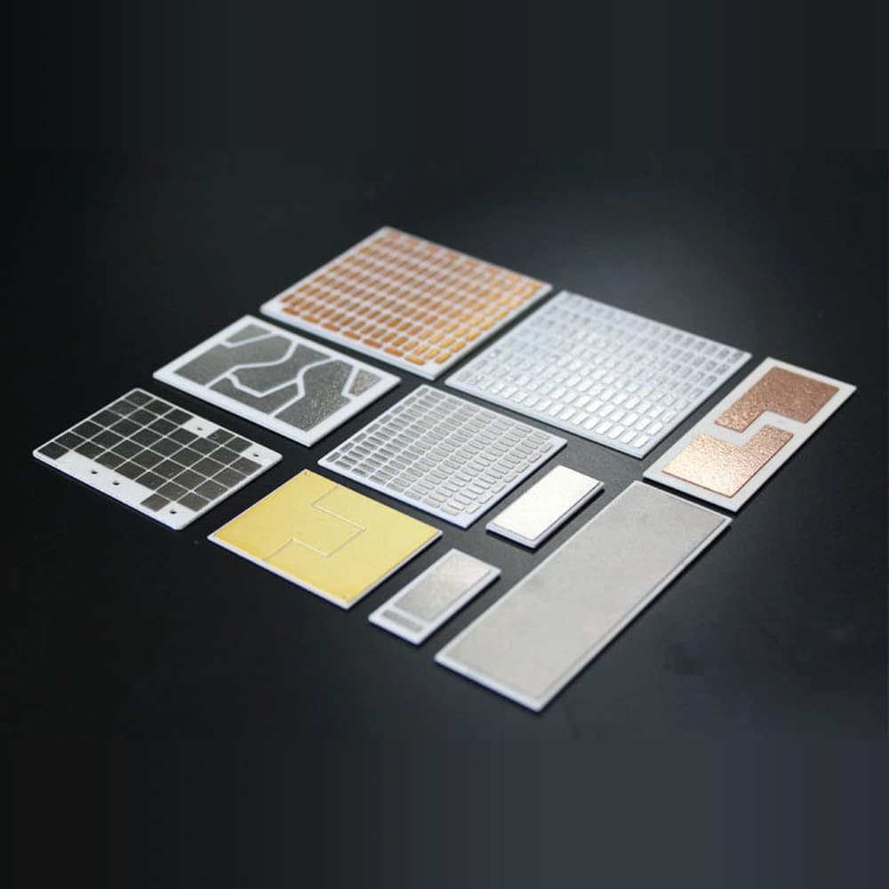
- Copper coverage, isolation gaps and usable outline coordinated within one etched pattern.
- Thermal-contact geometry treated separately from the AlN material conductivity.
Engineering Questions
Can I use the bare AlN temperature limit as the DBC operating limit?
No. Copper, interfaces, finishes, attachment materials and package construction can impose different limits. Use a qualification basis for the complete intended stack.
Is DBC just copper mechanically attached to ceramic?
No. DBC is a controlled high-temperature bonding technology, not merely mechanical attachment.
Why must copper thickness and circuit spacing be reviewed together?
Thicker copper changes the conductor cross-section and etched sidewall geometry. Confirm finished track width, isolation gap and edge clearances for the selected thickness rather than applying one spacing rule to every stack.
Packaging & Shipping
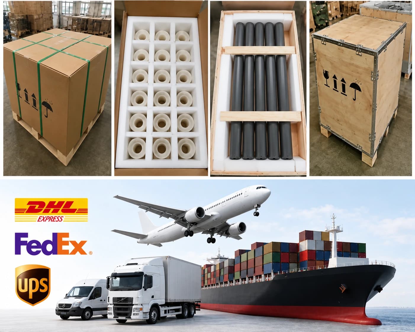
Packaging is selected for master cards, individual units and copper surface condition.
| Item | Details |
|---|---|
| Packaging approach | Packaging is selected for master cards, individual units and copper surface condition. |
| Protection methods | Individual separation; Anti-scratch surface protection; Rigid trays or master-card frames; Copper corrosion protection where appropriate; Inner box and export carton; Wooden case when required |
| MOQ reference | 5 pieces or one master-card equivalent |
| Lead-time references | DBC: 5-9 weeks |
| Payment terms | T/T / Western Union / PayPal; 50% advance payment, 50% balance before shipment |
| Shipping methods | Sea freight / Air freight / Door-to-door courier |
Related Ceramic Substrate Products
Compare related ceramic substrate materials and metallization routes within the same product family.